-
-
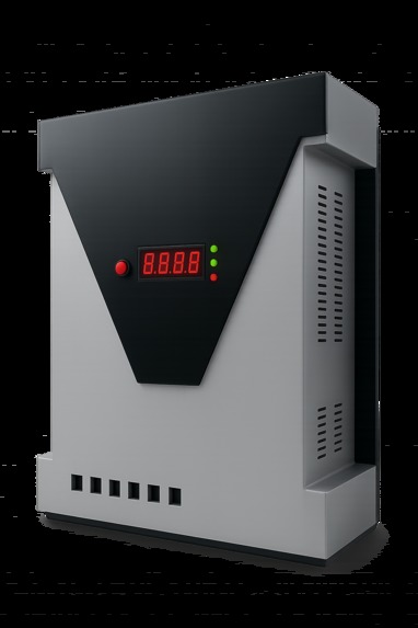
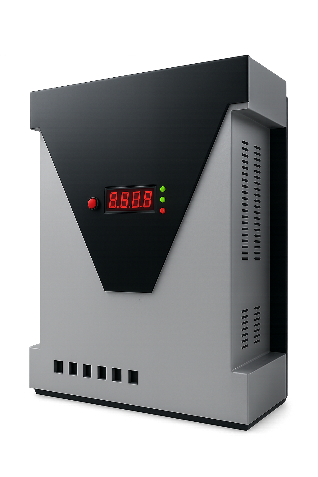
PREMAUDA Digital Pure Sine Wave Inverter/Charger
-
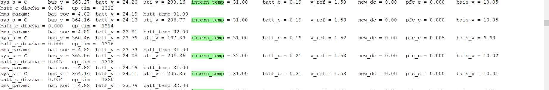
PuTTY serial output showing inverter system logs and real-time status feedback from C2000 microcontroller
-
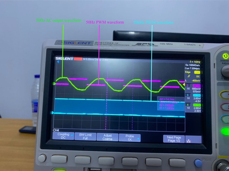
Oscilloscope Inverter output voltage, DC-AC PWMs showing Carrier and Modulation PWM (unipolar Pulse width Modulation))
-
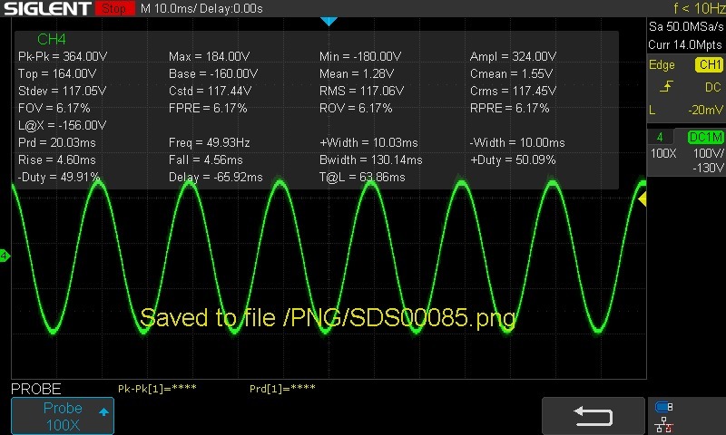
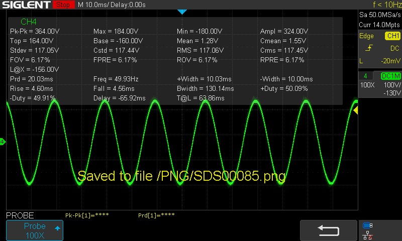
Oscilloscope Inverter Pure Sine Wave Output at 50Hz
-
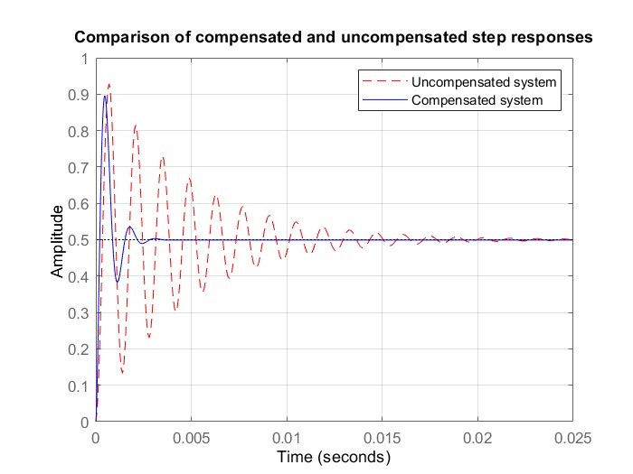
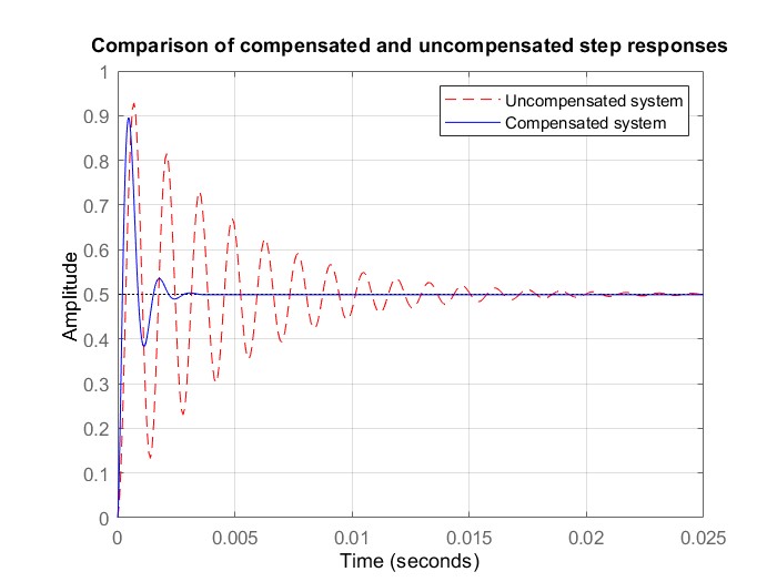
Step response of DC-AC control design (Matlab)
-
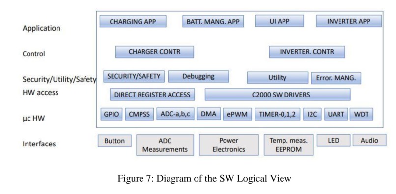
Software Design Logical View
-
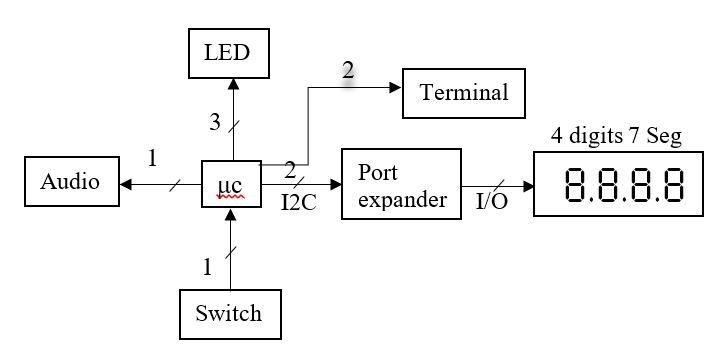
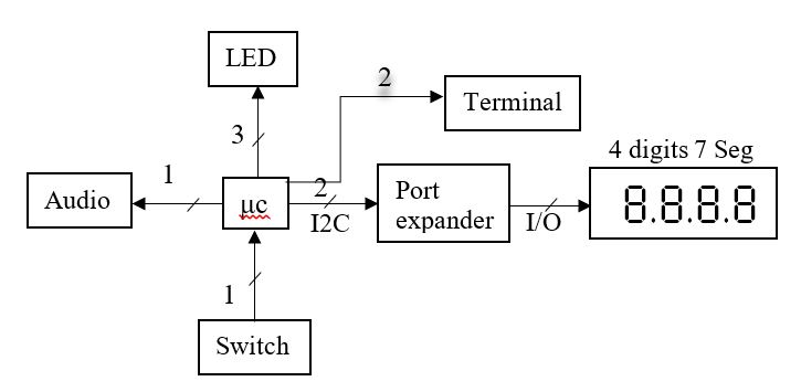
User Interface - Audio, led, switch, uart-serial terminal, i2c 7 segment display
-

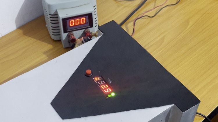
Our Build in Action
-
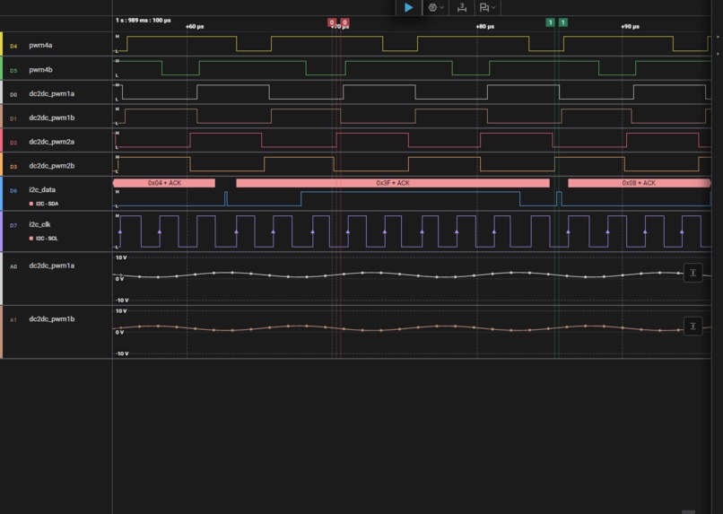
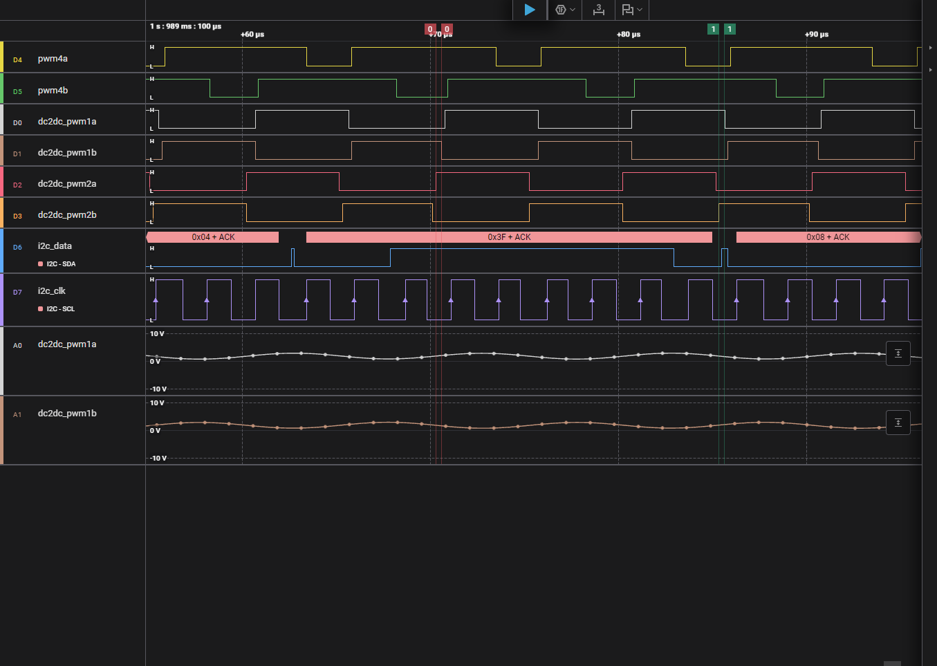
Logic analyser measurement of charger DC - DC buck (PSFB ) and 7 Segment i2c signal


Inspiration
Behind our product lies a vision shaped by four powerful drivers: the urgent energy challenges in Africa; the global shift toward renewables; the need to develop intelligent embedded technology which is made in Nigeria and a passion to apply engineering principles taught in classrooms to real-world problems. Each of these inspirations deeply influenced how we approached the design and development of our product. They include:
a. Energy Crisis: Nigeria and Africa have a dual problem of energy crisis and reliance on imported energy products as an alternative to energy supply from utility companies.
b. Focus on Renewable Energy: In line with SDG 7 (Affordable and Clean Energy) and SDG 13 (Climate Action), there is a global shift toward replacing fossil-based energy systems with cleaner, renewable energy sources. This transition is driven by urgent environmental goals, and our product directly contributes to this vision by supporting off-grid and hybrid solar energy systems that reduce dependence on diesel generators and fossil fuel-based electricity.
c. Advanced Technology: We decided to design a product that departs from traditional technology, hence a product that has an advanced real-time microcontroller at its center. This has several advantages over traditional and analogue power electronics systems and gives it wide range of application and smart functionalities.
d. Engineering Theories: We wanted to use the engineering we learnt in the university, hence a project that cuts across several aspects of engineering
Our Product - What it does
Our product is an important component in off-grid energy solutions and renewable energy systems. It has two main functions and several other auxiliary but important functionalities
Main functions
a. Inverter functionality: Our product produces a pure sine wave 220V AC output voltage at 50Hz. It converts either 12V/24V DC input voltage to 400V DC using a push-pull current-fed boost converter and then converts the 400V DC to 230V AC using a modified unipolar modulation DC-AC topology.
b. Charger functionality: Our product charges either a 12V/24V battery with an input AC voltage of between 150V - 240V. It first converts the AC voltage to 400V DC using an interleaved PFC/boost topology, after which it converts the 400V DC to 12V/24V using a Phase-Shift Full-Bridge topology DC-DC converter. It is capable of charging several types of batteries.
The technology in these two main functionality could be scaled for EV (electric vehicle) charging, merchant power supply systems and other power supply sytems.
Other Functions/features
c. Battery Management System: The firmware has a battery magement system that monitors the various charging and battery parameters, does temperature compensation, 3 or 4 stage charging based on the battery type, protection against overcurrent, overvoltage, overtemperature and short circuit faults, including computation of important battery parameters.
d. User Interface: The system comes with 5 user interfaces. These are: switch to turn on the inverter, LEDs to indicate the device state, audio to communicate with the user when far from the system and a 4-digit 7-segment display on an I2C bus to indicate important system parameters. A serial terminal is available for technicians to use to access the device in maintenance mode.
e. Protection: The device implements several protections for safe operation and system reliability and durability. This includes microcontroller silicon trip for fault conditions to protect the power electronics, soft start algorithm at PE start up and others.
f. Automatic battery type detection: At start up, the device automatically detects the type of battery (12V or 24V) connected to the system and based on this, the system loads the correct parameters that relates to the battery type for the device's proper functionality
g. Energy Management System: The system does other computation that relates to energy usage, hence providing the user with important information about their energy usage.
How we built it
The product was designed as an extensive engineering project. It involves all stages of developing an embedded product; these include project management, hardware, software and control design and implementation; testing and integration, supply chain activities, proper documentation, design alternatives and final decisions among others.
Various project implementation stages and activities are summarily enumerated below
A. Pre-design Stage
These were activities that preceded the commencement of the actual product design.
i. Research and Selection of power electronic (PE) topologies: Extensive research was done into various PE topologies before the final selections were made.
ii. Microcontroller selection and SW design tools: Microcontrollers (μc) from various μc manufacturers were reviewed before the selection of the TI C2000 platform.
iii. Project Management: Extensive project management was involved in the project. Monthly meeting, stand-up scrum and resource allocation.
iv. System specification: The product and subsystem specifications were decided upon. A listing is presented below in Table 1
Table 1: The Inverter/Charger System Specifications
General
| Parameter | Inverter | Charger |
|---|---|---|
| Input (V) | 12V / 24V DC | 230V AC |
| Output (V) | 230V AC | 12V / 24V DC |
| Frequency (Hz) | 50Hz | – |
| Current (A) | 2.5A | 20A |
| Power Rating | 600W | 400W |
DC-DC Converter
| Parameter | Inverter | Charger |
|---|---|---|
| Topology | Current-fed Push-Pull | Phase-Shifted Full Bridge (PSFB) |
| Control | ACMC | PCMC |
| Input (V) | 12V / 24V DC | 380V – 400V DC |
| Output (V) | 375V – 400V DC | 12V / 24V DC |
| Switching Freq. | 100kHz | 100kHz |
DC-AC Converter/PFC Converter
| Parameter | Inverter | Charger |
|---|---|---|
| Topology | Modified Unipolar Modulation | Interleaved Boost |
| Control | PR Controller | ACMC / PI |
| Input (V) | 380V DC | 150V – 265V AC |
| Output (V) | 230V AC | 400V DC |
| Output Freq. | 50Hz | – |
| Switching Freq. | 20kHz | 100kHz |
B. Product design phase
This phase encompasses a range of activities, including decisions on the theories and PE topologies to be used, calculations based on these decisions, all HW and control calculations, SW design, various implementations and testing. Brief details are listed below:
i. HW: This encompasses several steps such as PE topology selection and calculation, measurement circuits design, HW unit and sub-systems design, Simulation of designs, breadboarding and PCB breakout board design for testing. Microcontroller selection, pin mapping and integration of microcontroller to the hardware circuit was also done.
ii. Software: Firmware plays a very important role in all embedded systems. The SW architecture was designed with the firmware written in C++. An in-depth understanding of the microcontroller was accrued to enable us to program it successfully, after which the SW unit implementation and testing were done.
iii. Control system: Several digital controls were designed to ensure the product operates in a consistently stable state. The control system output is converted to duty cycle/PWM, which drives the power electronics to generate the required voltages. The control system tasks included control type selection, modeling and design, simulation using MATLAB, control logic implementation and final HW & SW integration into the overall system.
iv. Testing and System Integration: Testing and system Integration is an important aspect of embedded system design. This includes unit, module, sub-system and system testing and integration.
v. Others
• Mechanical design
• Supply chain activities.
We utilized a range of hardware tools to aid in the design, testing, and verification of our embedded system and power electronics prototypes, which are listed in Table 2.
Table 2: List of tools used for development
HW Tools
| S/N | Tool Name | Usage |
|---|---|---|
| 1 | Logic Analyzer | View/inspect microcontroller signals, serial bus signals |
| 2 | Oscilloscope | View and analyze analog and digital signals |
| 3 | Electronic Load | Simulate load conditions for testing |
| 4 | Eagle CAD | Draft hardware circuits and design PCBs |
| 5 | LT Spice | Simulate electronic hardware designs |
SW Tools
| S/N | SW Tool Name | Usage |
|---|---|---|
| 1 | GIT | Version control for software development |
| 2 | MATLAB/Simulink | Testing and simulation of control loop designs and PE topology |
| 3 | TI Code Composer Studio | IDE for firmware development and debugging |
| 4 | TI Proprietary Tools | Simulation of power electronics (PE) topologies |
Challenges we ran into
Several challenges and constraints were encountered in the design of the product, some are listed below:
1. Resource Limitations in Embedded Systems
When compared to desktop-based systems, embedded platforms have limited processing power, constrained memory, and strict timing measurements. This required rigorous code optimization, especially for a fully digital product like ours, with over 15,000 lines of code. The use of lightweight control algorithms, all made under tight real-time constraints, must be factored into the design process.
2. Component Sourcing
Key hardware components were not locally available and had to be sourced internationally, which was challenging. This introduced occasional lead times, additional development costs and occasionally design revisions in order to accommodate available substitutes while maintaining system integrity.
3. Digital Control of Power Electronics System
Implementing precise Digital Control of Power Electronics Systems is a complex field of control that requires more than just theoretical understanding but an in-depth knowledge and expertise in control loops, signal conditioning and noise immunity.
4. Standard for high frequency Power Electronics Devices
Standard design practices in both embedded systems and PE placed structural constraints on architecture selection, thermal management, isolation techniques, and Electromagnetic Compatibility (EMC). Integrating these diverse requirements into a compact, cost-effective prototype pushed the boundaries of our design flexibility.
5. Test and Lab set up
The final validation of such a system demands high-grade test equipment, including oscilloscopes, programmable power sources, electronic load banks, PCB machine, which are expensive for a start-up.
Performance and Test Benchmarks
Table 3: Inverter Performance and Benchmark Tests (with expected results)
a. IEC 62109 – Electrical Safety & Thermal Performance
| S/N | Test Category | What to Test | Expected Result | Actual Result | Remark |
|---|---|---|---|---|---|
| 1 | Startup Behaviour | Soft start, buzzer/display feedback | <2s startup, display and buzzer active | LED and 7 segments come on, buzzer sounds on boot | Pass |
| 2 | Overload Protection | Reaction to overload | Safe shutdown at 110% load | Safe Shutdown | Pass |
| 3 | Reverse Polarity | Reverse battery terminal input | No boot, buzzer or LED alert | Buzzer beeps, No boot | Pass |
| 4 | Temperature Test | Fan, Surface/heat sink under load | 45–65°C at load | temperature okay and shutdown at over temperature | Pass |
| 5 | Audible Noise Level | Inverter/fan noise under operation | Low hum acceptable | Quiet operation | Pass |
b. REA/NEMSA Nigeria – Grid-aligned Mini-grid Inverter Standards
| S/N | Test Category | What to Test | Expected Result | Actual Result | Remark |
|---|---|---|---|---|---|
| 6 | Output Voltage Stability | AC output under different loads | 220–230V | 220.8V | Pass (device can handle between 100V - 265V AC Volts) |
| 7 | Output Frequency | Frequency at no/full load | 50.0 Hz ± 0.2 Hz | 49.95Hz under load and 50Hz under no load | Pass |
| 8 | Load Switching Response | Bulb/fan switching impact | Bulb remains stable | No flicker observed | Pass |
| 9 | Battery Protection | Low voltage cutoff, reverse blocking | Shutdown <10.9V, battery reverse polarity protection | Auto cutoff at 11.0V, battery reverse safe | Pass |
c. Oscilloscope output screenshots
The following figures illustrate the inverter’s conditions, as captured by an oscilloscope:
Figure 1:Inverter PWM Duty Cycle and AC Output Waveform of DC–AC Converter Charger PWM output
Figure 2: Unipolar modulation Inverter PWM Waveform Duty Cycle of DC–AC Converter Unipolar modulation PWM Waveform
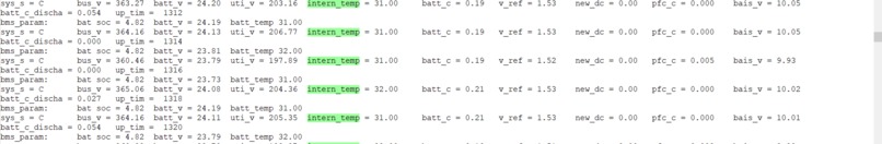
Figure 3: Serial Terminal debug output Serial Terminal debug output
Legend
Sys_s - system state; C – charging; bus_v – bus voltage; util_v – utility voltage; batt_c – battery current; v_ref – voltage reference; pfc_c – power factor correction current; bias_v – bias voltage; batt_c_discharge – battery current discharge; up_tim -up time; bat soc – battery state of charge
Figure 4: User Interface User Interface
d. Video of our build in action Build in action
Our Proud Engineering Accomplishments
This is our second product under the Low Power Energy Systems category in the company’s short-term roadmap, following the successful development of our MPPT Solar Charge Controller.
1. Built from scratch: Local Innovation, Global standards: Successfully designed in-house (Made in Nigeria) a complete and complex embedded system for a Digital Pure Sine Wave Inverter/Charger with closed-loop digital control, built from scratch to meet international standards, unlike traditional alternatives in the market.
2. Complete Local Hardware design and assembly: All circuit and PCB design was carried out locally, without outsourcing, showcasing our full-stack hardware development capability.
3. Reliable and Robust Firmware: Developed robust firmware in C++ capable of handling a wide range of operational conditions and fault conditions reliably.
4. Complete in-house Embedded Engineering: Tackled the full embedded product lifecycle: selected and implemented a complex microcontroller, designed its hardware interface, developed and deployed its software architecture, engineered the control system, and integrated all components into a functioning product.
5. Future-ready and scalable for EV charging system: Our product topology and functionality is suitable for L1 and L2 EV charging; on board charger and Electronic Vehicle Service Equipment (EVSE) design. Scaling and minor module additions to the design would enable us to design such EV charging systems easily.
6. Class room engineering theory in action: It's rewarding to see classroom concepts like control theory and system modelling translated into real-world software. More than just an inverter/charger, this project reflects our growing expertise in complex embedded system design, preparing us for even more advanced product development in the future.
7. Project artifacts:
We are proud of the project 5 product deliverables which we are at 90% completion. These are:
i. Professional software development process/project
ii. Product Firmware
iii. Standard circuit diagram
iv. PCB of design
v. Product prototype.
What we learned
The experience we have gained from the project is numerous. A listing of some are below:
1. Embedded product design: We learnt how to design an embedded product - from concept through the various engineering design and implementation phases to the product realisation phase.
2. Digital Control: Implementation of digital control systems in embedded systems was carried out, and this greatly enhanced the team's knowledge of this complex field of electrical engineering.
3. Project management: A complex project calls for successful project management in terms of tasks allocation, maximizing manpower, project resource allocation, and scrum usage.
4. Software Engineering: Designing software for an embedded product does not mean just knowing a programming language or simply writing code, but rather, the software has to be properly designed and thought through before coding begins. For embedded software, a good understanding of the hardware design is also needed. This was a skill learnt by the team members.
5. Usage of Software and Hardware tools: Several tools are needed for the successful development of an embedded device, some of the tools used are: GIT for software version control, LT-Spice for circuit design simulation, and MATLAB for testing of control designs.
6. Mastery of electronics laboratory equipment: The project provided hands-on experience with essential laboratory equipment, deepening our understanding of their practical applications. We gained proficiency in using tools such as oscilloscopes for signal analysis, logic analyzers for debugging communication protocols, and electronic loads for simulating real-world power consumption. This mastery enabled us to validate circuit behaviour, troubleshoot complex hardware issues, and improve the overall quality of our hardware development process.
7. Deep knowledge of TI TSM320F2800049c real-time microcontroller: The microcontroller is a complex DSP which can be used in several white goods products, and several peripherals of the microcontroller were used to design our product.
8. Knowledge for next power electronics Project: The technology in the product has prepared the start-up for any next power electronics product, be it for an EV charging, an industrial inverter, or a dishwasher. The technology in these products was learnt in the process of designing our first product.
What’s Next for the Digital Pure Sine Wave Inverter/Charger
Our Digital Pure Sine Wave Inverter/Charger is the second product in our Low Power Energy Systems product line. This series includes:
• A Solar Charge Controller (already completed and undergoing field trials),
• The Digital Pure Sine Wave Inverter/Charger, and
• A Smart Hybrid Inverter that combines a solar charge controller, inverter, and utility charger (3in1) into one compact
system (currently in development).
Next Steps:
1. Complete Integration & Field Testing
Finalize the integration of all sub-systems and deploy the product to a customer site for extended real-world testing.
2. Scale-Up & Smart Hybrid Development
Use the current inverter/charger design as a platform to develop a higher-capacity version. This will serve as the base for our upcoming Smart Hybrid Inverter (3-in-1) system, which integrates MPPT charge control, battery charging, and power inversion in a single unit.
3. Pursue Funding for Mass Production
To bring this product to market at scale, we are actively exploring funding sources, including grants, private investors, and bulk purchase commitments from major customers.


Log in or sign up for Devpost to join the conversation.