Inspiration
Artificial intelligence is what everyone at this event is building around, but almost none of the surrounding conversation touches the physical layer underneath it, the fabrication and verification of the chips that make any of it run. As a nanotechnology engineering student with hands-on wet lab fabrication experience, and as someone who already works as a Quantum Outreach Educator introducing complex physics to public audiences, I wanted to build something that makes that invisible layer tangible for people encountering it for the first time.
The AI infrastructure depends on a chip supply chain currently bottlenecked by manufacturing and metrology capacity rather than by demand. GPU lead times are running 36 to 52 weeks, and HBM memory is reportedly sold out through 2026. Very few people outside semiconductor circles know that an entire category of instrument exists whose only job is checking that a fabricated feature on a wafer came out to the correct depth, and that this checking step is itself part of the bottleneck.
I wanted this project to introduce people to that world directly: handing them a working instrument from that same category and letting them watch it measure something live. I considered building toward atomic-resolution imaging with a scanning tunneling microscope, and ultimately chose to build a contact stylus profilometer instead, the same broader category of instrument fabs use for process verification, because it let me deliver something fully working, explainable, and buildable within this short time frame.
What it does
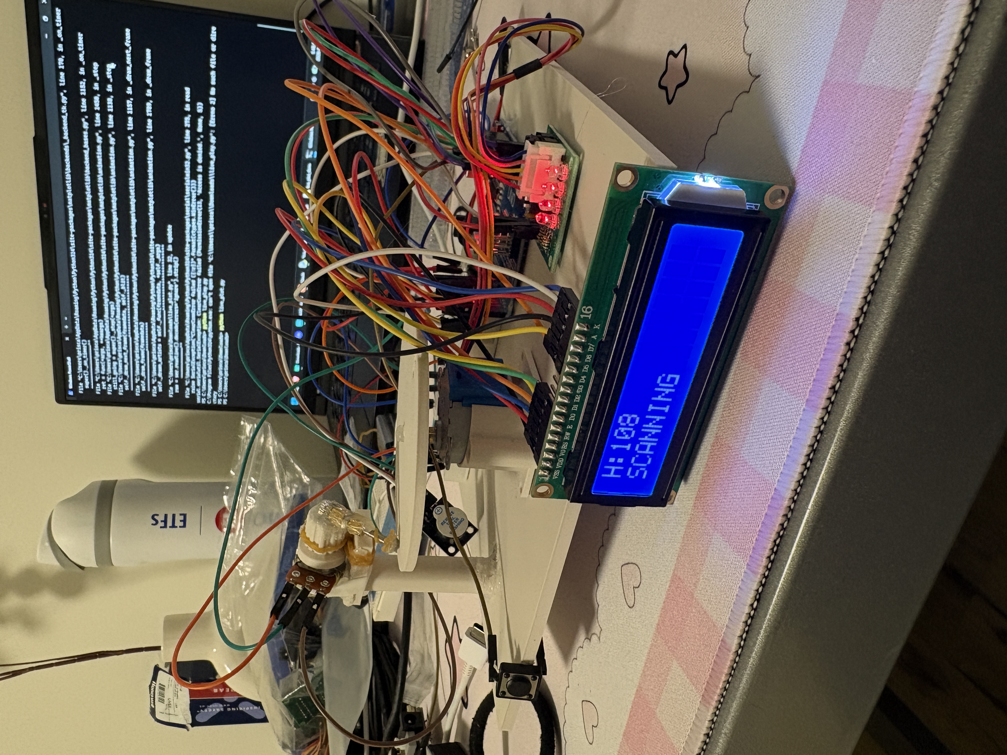
Fabs use contact stylus profilometers to verify that an etched feature on a wafer came out to the correct depth. $66,090 is a working version of that instrument.
A stepper motor spins a 3D-printed disc with a trench of known depth cut into its surface. A stylus stays fixed in place, resting lightly on top of the disc, and once per rotation the trench passes beneath it, causing the stylus to dip.
That dip is a mechanical deflection. It rotates a potentiometer's shaft, which produces a voltage, which an Arduino reads and streams out over serial in real time.
A Python script plots that stream live, so the exact instant the stylus finds the trench appears as a visible dip on screen, synchronized with an LCD status readout and an audible tone. Every value on that plot is a physical measurement, not a simulation.
How I built it
I designed and 3D printed five custom structural parts in PLA: a base plate, a support column, a cantilever arm, a stepper motor mount, and a turntable disc.
The potentiometer is mounted with its shaft oriented horizontally, so that deflection of the stylus arm rotates the shaft rather than swinging past it. Rotation comes from a 28BYJ-48 stepper motor driven through a ULN2003 module.
An Arduino Uno handles motor sequencing, sensor reads, an LCD status readout, and a buzzer cue, and streams that data over serial to a Python and Matplotlib script that renders the live plot shown to the audience.
Challenges I ran into
Getting the stylus itself to reliably transmit force into the shaft, rather than simply flexing in place, took mechanical iteration, a rigid screw tip and rubber band tension in place of a bare bent wire.
Accomplishments that I'm proud of
I built and debugged a complete system in a single overnight session, spanning mechanical design, electronics, firmware, and live data visualization.
Every number that appears on the live plot is sensor data from the physical build, not a simulation. That distinction mattered to me throughout, and I held to it even when a shortcut was available that would have made the project look more capable than it actually is.
What I learned
Building an instrument in this category taught me the terminology and mechanics of contact profilometry far more effectively than reading about it would have.
I also learned that a smaller, fully honest, fully working build holds up under scrutiny in a way that an ambitious but unverified claim does not, and that it is worth accepting that trade-off early rather than discovering it under pressure during judging.
What's next for $66,090
- Attempting the original STM electronics with properly sourced components
- Adding a multi-depth calibration disc to demonstrate accuracy across several known values instead of just one
- Replacing the mechanical potentiometer with contactless Hall-effect sensing to remove the wire-transmission uncertainty entirely
- Integrating this work as a complementary measurement mode within a larger project already in progress, an automated optical wafer and MEMS inspection platform
Built With
- arduino
- autodesk-fusion-360
- c++
- matplotlib
- pyserial
- python


Log in or sign up for Devpost to join the conversation.