-
-
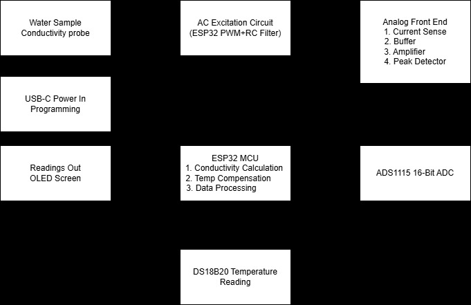
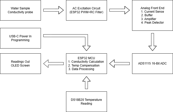
System architecture flowchart
-
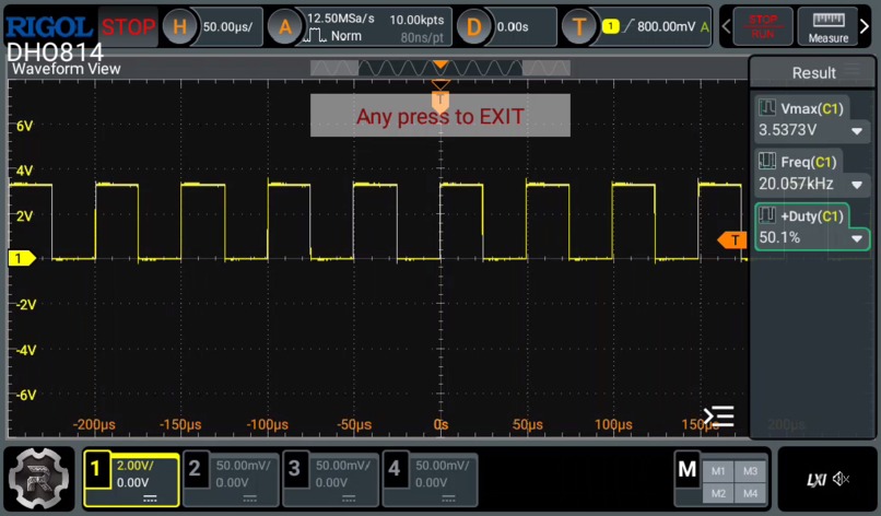
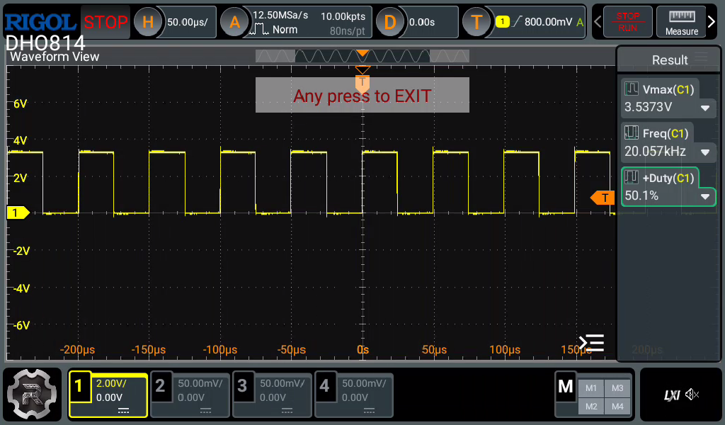
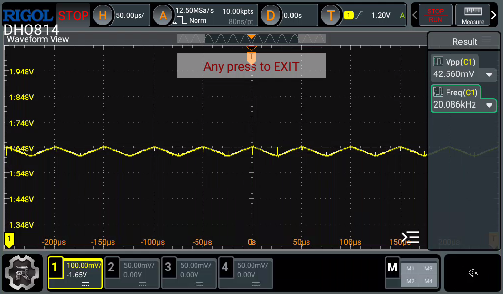
20KHz excitation signal generated by the ESP-32
-
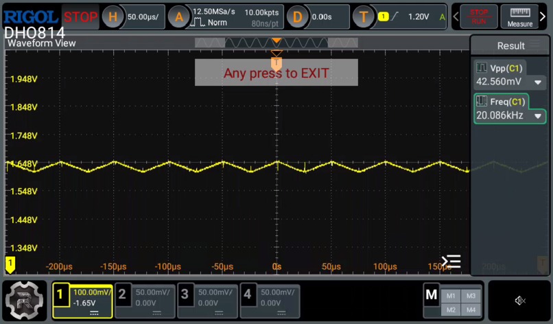
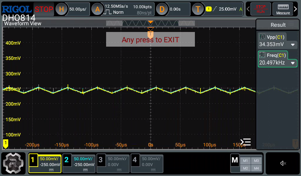
R-C filter output signal
-
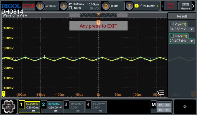
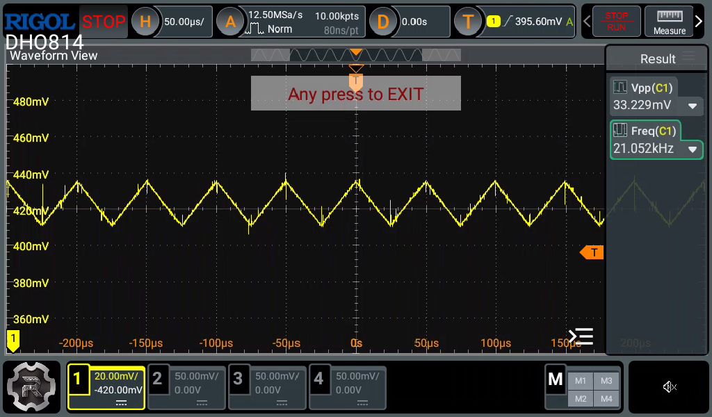
Buffer output, Blue wave is the buffered signal received, for testing, both probes were connected together (only this pic)
-
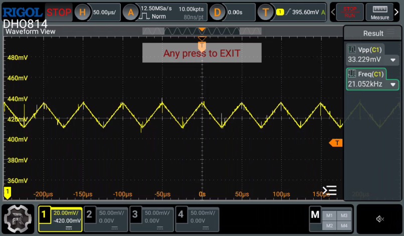
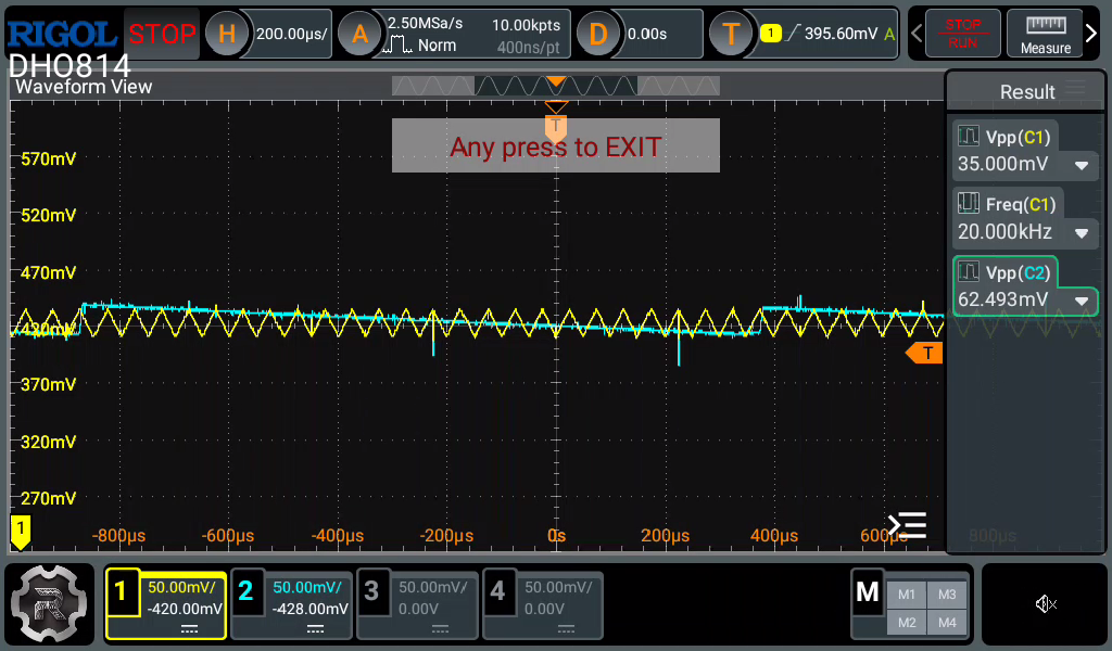
Amplified output of the buffered signal (Here we are using an equivalent resistance of 1K to simulate brackish water for this test)
-
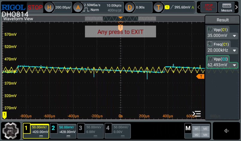
Peak detector output (Blue) Vs Amplified Signal(Yellow) for the Brackish water equivalent resistance test
-
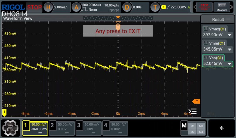
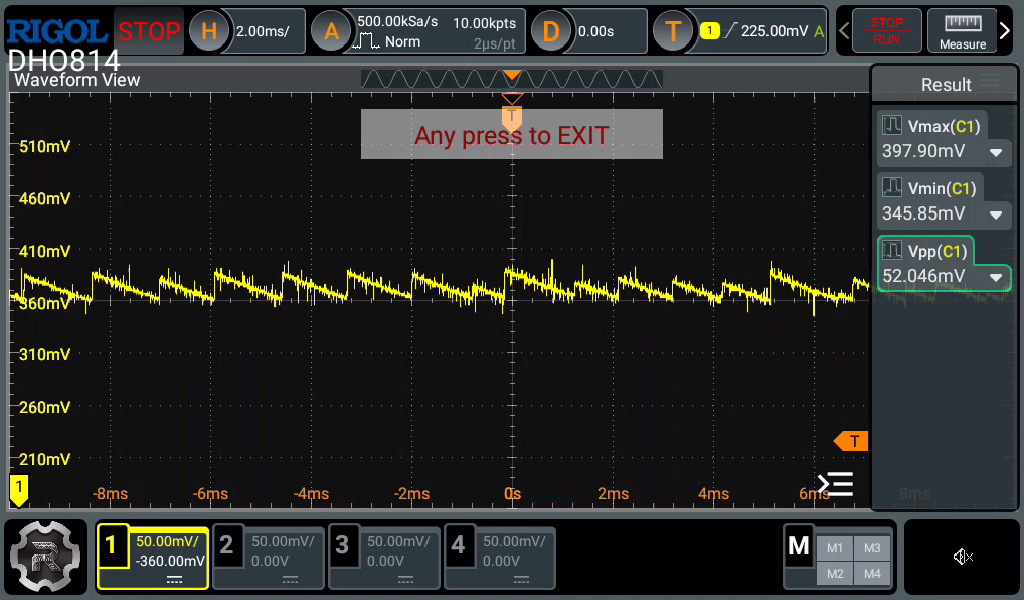
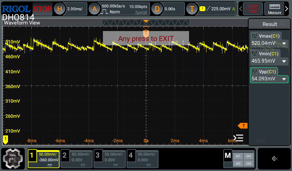
Peak detector output when normal tap water is used (actually tested)
-
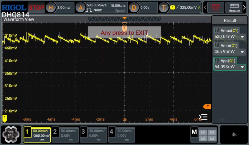
Peak detector output when salty water is used (actually tested)
-
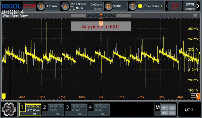
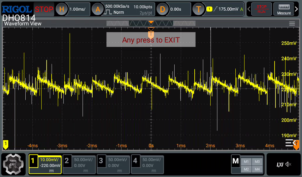
Peak detector output at equivalent resistance of 8.2K ohm resistance, equivalent conductivity for k=1cm^-1 detected is 122uS/cm
-
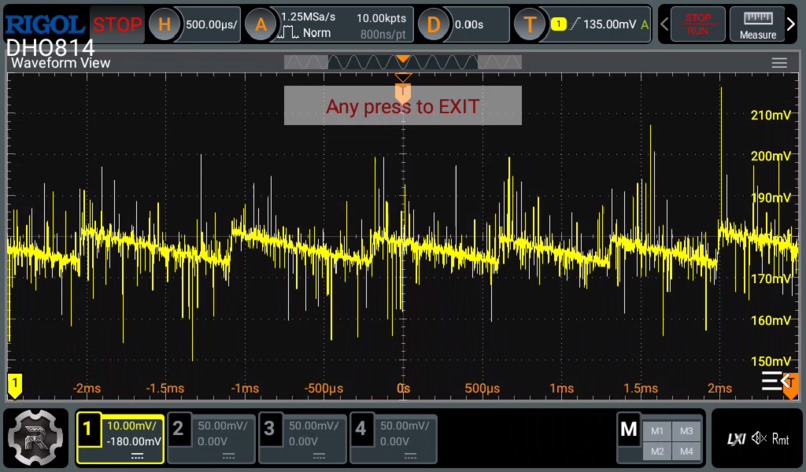
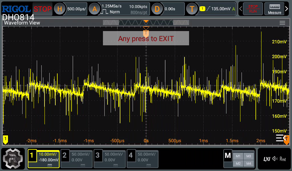
Peak detector output at equivalent resistance of 12K ohm resistance (for equivalent conductivity k =1cm^-1 is 83.3 uS/cm)
-
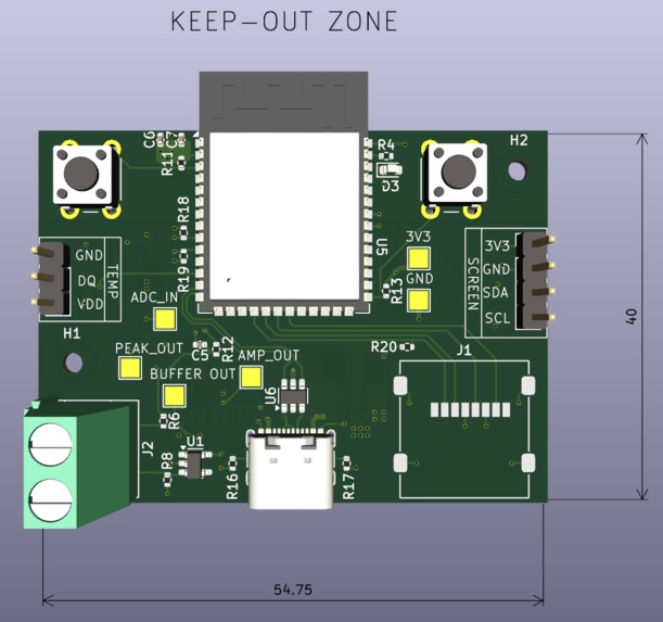
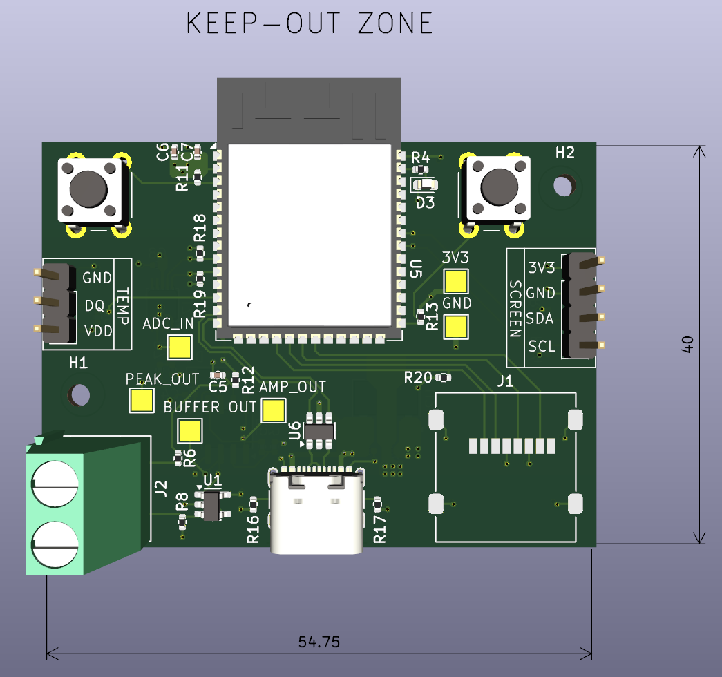
Front PCB render
-
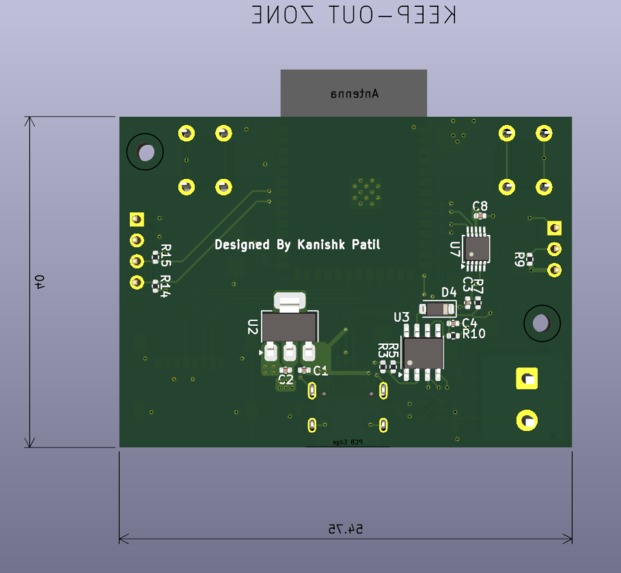
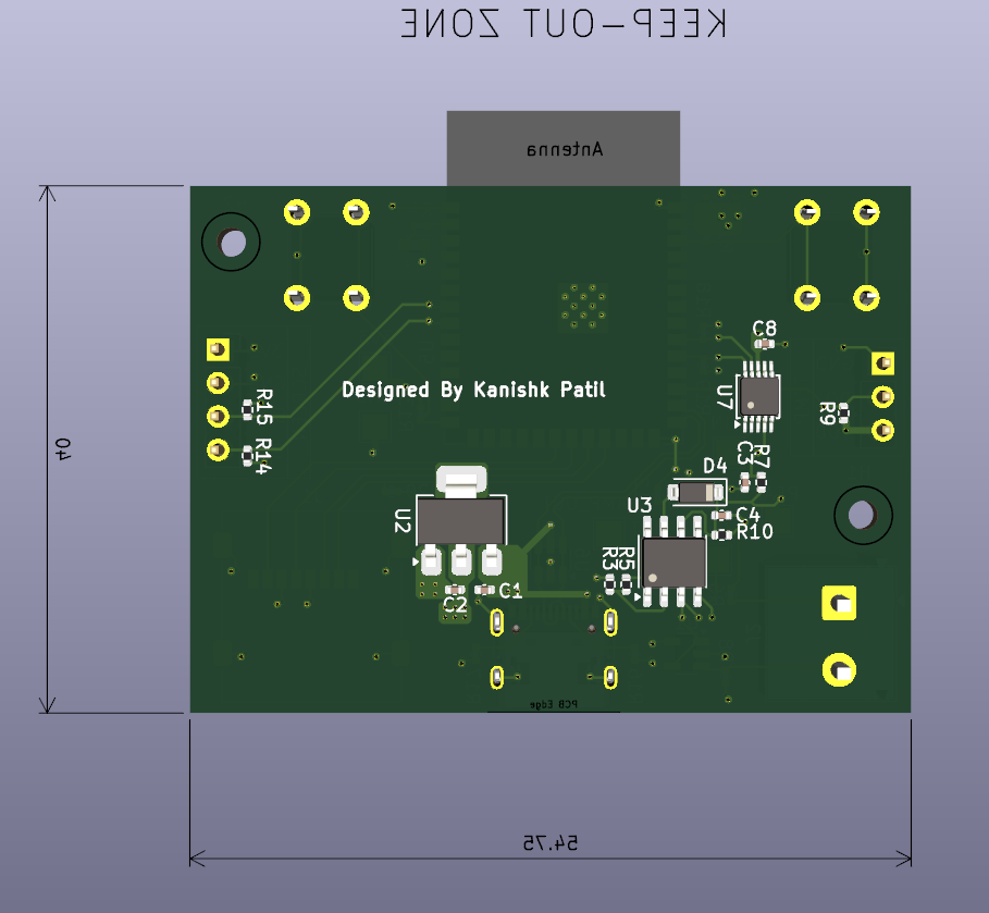
Back PCB render
-
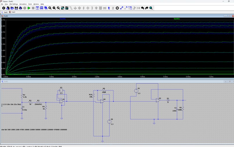
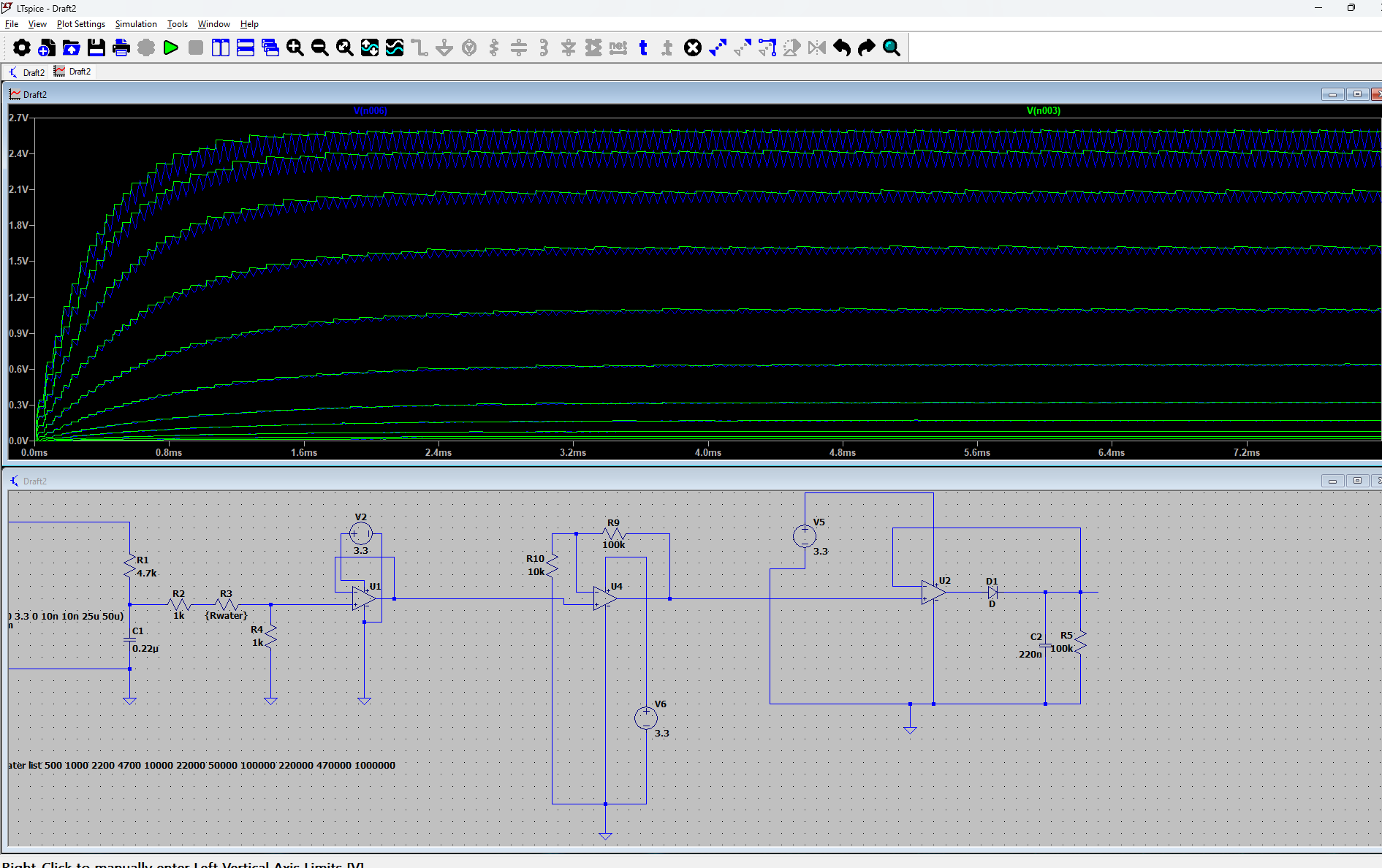
ADC verification resistance sweep in LTSpice, along with analog front end simulation pic
-
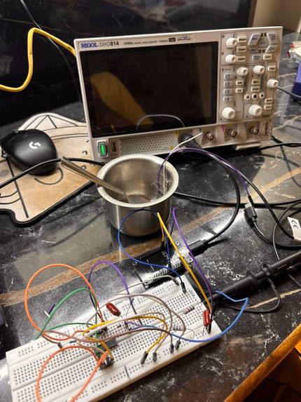
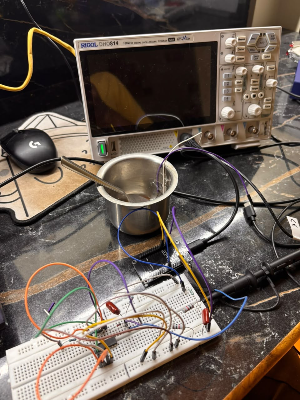
Setup used for testing purposes
Portable Temperature-Compensated Conductivity Meter
Inspiration
I wanted to build a real measurement instrument from the ground up rather than treating a sensor as a black box.
As a Chemical Engineering student moving toward embedded systems, instrumentation, and process control, conductivity was a natural problem to work on. It is a useful measurement in water-quality and process-water applications, but the interesting part for me was not simply getting a conductivity value on a screen. I wanted to understand the entire chain between a physical property of water and the digital number an instrument reports.
That meant learning how to handle the sensor excitation, tiny analog signals, signal conditioning, analog-to-digital conversion, temperature effects, calibration, and embedded processing as one system.
The project started as a question:
What would it actually take to build a conductivity meter instead of just buying one?
It turned into a much bigger engineering exercise.
What We Built
The Rev1 prototype is a portable conductivity measurement system built around an ESP32-S3.
The measurement chain is:
Conductivity cell → AC excitation → analog signal conditioning → rectification/peak detection → external ADC → digital processing → temperature measurement → conductivity calculation
The controller is an ESP32-S3-WROOM-1-N8R8.
The conductivity measurement uses an approximately 20 kHz AC excitation signal rather than a simple DC measurement approach. The analog circuitry conditions the resulting signal before it reaches an ADS1115 16-bit ADC.
A DS18B20 is included for temperature measurement so that the system can ultimately report temperature-compensated conductivity.
The broader Rev1 design also includes an OLED interface, data logging, power regulation, and a dedicated 4-layer PCB designed in KiCad.
For Rev1, the working electrical reference is a cell constant of K = 1 cm⁻¹.
The Measurement Principle
Conductivity is related to conductance:
$$ G = \frac{1}{R} $$
and, for a conductivity cell:
$$ \kappa = K G = \frac{K}{R} $$
where:
Ris the effective resistance measured through the cellGis conductanceKis the cell constantκis conductivity
This relationship looks simple on paper, but the actual measurement is not.
The physical probe, excitation waveform, analog front end, temperature, cell geometry, and calibration all influence the final result.
That was one of the reasons I chose to build the instrument myself: the project forced me to understand the difference between the equation and the real measurement system implementing it.
Designing the Electronics
The first version of the architecture was developed in LTspice before being assembled on a breadboard.
The system was designed around several key decisions.
AC excitation
The conductivity cell is driven with an AC signal at approximately 20 kHz rather than relying on a simple DC resistance measurement.
The excitation is generated from the ESP32-S3 and conditioned for the analog measurement path.
Analog conditioning
The signal produced by the conductivity measurement can be small, so it needs to be buffered, amplified, and converted into a form that the ADC can use reliably.
The physical breadboard implementation uses an LM324-based analog front end with approximately 2× gain.
External ADC
The ADS1115 provides a dedicated 16-bit conversion stage instead of making the conductivity measurement depend entirely on the ESP32's internal ADC.
Temperature sensing
The DS18B20 provides the sample temperature required for temperature compensation.
Digital output
The processed measurement is intended to be displayed and logged digitally, making the system more useful as an instrument rather than just an analog experiment.
Simulation Before Hardware
LTspice was used throughout development to investigate the circuit before and during hardware testing.
I simulated:
- the buffer stage
- resistance sweeps
- signal amplification
- rectification
- peak detection
- expected output behaviour
The simulations were useful for understanding expected signal levels and deciding which component values and circuit approaches were worth trying on hardware.
They also exposed an important limitation of simulation:
A circuit that looks correct when driven by an ideal source does not necessarily behave the same way when it is connected to the entire real measurement system.
The First Major Challenge: A Very Small Signal
One of the first practical problems was signal amplitude.
At some equivalent resistances, the useful measurement signal was only in the millivolt range.
That meant the ADC could not simply be connected directly to the probe and expected to produce a useful measurement.
The analog front end had to provide enough gain and signal conditioning while still operating correctly around the single-supply virtual-ground architecture.
This forced me to think about the complete analog path rather than designing each block independently.
When Simulation and Hardware Disagreed
The precision-rectification stage was one of the most difficult parts of the project.
A rectifier topology behaved correctly in a simplified simulation using an ideal sine wave.
When integrated with the actual biased measurement system, however, the behaviour was significantly less ideal.
The interaction with the approximately 1.65 V virtual-ground reference became important, and the real sensing environment exposed problems that were not obvious from the simplified simulation.
The solution was not to assume the simulation was wrong or the hardware was wrong.
Instead, the circuit was broken down and tested stage-by-stage.
The development process became:
simulate → build → measure → compare → identify the mismatch → modify → test again
This was one of the most important lessons of the entire project.
Breadboard Reality
The first hardware implementation was built on a breadboard.
That made rapid iteration possible, but it also introduced problems that did not appear in simulation.
I encountered:
- electrical noise
- ripple
- wiring sensitivity
- grounding issues
- parasitic effects
- unstable-looking waveforms
- differences between simulated and measured behaviour
At times the waveform looked bad enough that the obvious conclusion was that the circuit had failed.
The oscilloscope showed otherwise.
By probing different points in the signal chain, I could separate problems in the actual circuit from artefacts caused by the measurement setup.
That was a major shift in how I approached debugging.
Learning to Use the Oscilloscope as Part of the Instrument
I used a RIGOL DHO814 oscilloscope to validate the prototype.
Instead of relying on a single final number, I used the scope to inspect the system at different stages:
- excitation
- conditioned signal
- amplified signal
- peak-detector output
- response to different equivalent resistances
One unexpected lesson was how much the measurement instrument itself can influence interpretation.
Some apparently unstable displays were related to trigger behaviour rather than the circuit signal itself.
That forced me to distinguish between:
signal behaviour
and
how the oscilloscope chooses to display that signal.
That sounds obvious in hindsight, but learning it experimentally was valuable.
Controlled Electrical Tests
Before testing real water, I needed a controlled way to change the electrical conditions seen by the measurement chain.
I therefore used known resistors as equivalent measurement loads.
For Rev1, using the working reference:
K = 1 cm⁻¹
the equivalent conductivity is:
$$ \kappa = \frac{1}{R} $$
Some of the experimentally tested points were:
| Equivalent Resistance | Equivalent Conductivity for K = 1 cm⁻¹ |
|---|---|
| 8.2 kΩ | ≈ 122.0 µS/cm |
| 12 kΩ | ≈ 83.3 µS/cm |
| 22 kΩ | ≈ 45.5 µS/cm |
| 33 kΩ | ≈ 30.3 µS/cm |
These are electrical reference points, not calibrated liquid measurements.
The purpose was to verify that the analog measurement chain produced a repeatable and monotonic response as the equivalent resistance changed.
The 8.2 kΩ Measurement
At approximately 8.2 kΩ, the oscilloscope showed a clear peak-detector output.
For K = 1 cm⁻¹:
$$ \kappa \approx 122.0\ \mu S/cm $$
This became one of the useful reference points for the physical prototype.
The important result was not the absolute conductivity number.
It was that a known electrical condition produced a measurable response through the full analog chain.
Extending the Test
The same approach was then used at approximately 12 kΩ and 33 kΩ.
Those correspond to:
- 12 kΩ → ~83.3 µS/cm equivalent
- 33 kΩ → ~30.3 µS/cm equivalent
for K = 1 cm⁻¹.
This extended the demonstrated electrical operating region and helped establish that the response was not limited to a single convenient test point.
From Resistors to Real Water
Once the electrical behaviour had been demonstrated, I moved to real water.
This introduced another important distinction.
A resistor is controlled.
Water is not.
The conductivity of a real sample depends on its dissolved ions, concentration, temperature, electrode geometry, electrode condition, excitation conditions, and other factors.
Because the system had not yet undergone proper calibration against known conductivity standards, the water experiments were treated as functional demonstrations, not absolute conductivity measurements.
Tap Water
Tap water provided the first simple real-world test.
The probe was placed in the sample and the conditioned analog output was observed.
The purpose was to confirm that the complete measurement chain could respond to an actual conductive liquid and not just to resistor substitutions.
Salt-Water Test
The most obvious real-world demonstration came from increasing the conductivity of the water by adding salt.
The initial water produced an output in roughly the 450–470 mV region.
After adding salt, the measured peak-detector output increased to roughly 520 mV, and after additional salt it rose to approximately 570 mV.
The important observation was the direction of change:
Increasing dissolved ionic content increased conductivity and produced a higher measured output.
This matched the behaviour expected from the measurement architecture.
The test was deliberately not treated as a calibrated conductivity measurement because the salt concentration, temperature, cell constant, and calibration chain were not controlled to laboratory standards.
Choosing the Cell Constant
During development, I initially considered how to make the instrument useful across a very wide range of conductivity.
That led to an important design decision.
For Rev1, I chose a fixed working reference of:
K = 1 cm⁻¹
This keeps the first version focused on proving the measurement electronics and producing a useful process-water-oriented prototype.
For Rev2, the architecture can be expanded to support selectable or custom cell constants with physically appropriate conductivity cells.
An important lesson here was that the cell constant is not just a software setting. The physical electrode geometry determines it; firmware can then use the correct value when converting measured conductance into conductivity.
Why Temperature Compensation Was Included
Conductivity changes with temperature.
Ignoring temperature would therefore make the measurement dependent not only on the sample but also on its temperature.
That is why the design includes a DS18B20 temperature sensor.
The intended chain is:
measure conductivity → measure temperature → apply the selected compensation model → report conductivity at the chosen reference condition
The Rev1 project establishes the hardware needed for this process.
A complete calibration and temperature-coefficient characterization are part of the next stage.
PCB Development
After the breadboard work, I moved the design toward a dedicated PCB in KiCad 9.
The Rev1 board is a compact 4-layer PCB, approximately 7.5 × 6.5 cm.
Moving to a PCB introduced another engineering layer.
The design had to consider:
- analog and digital sections
- grounding
- power distribution
- signal routing
- sensitive measurement nodes
- excitation coupling
- regulator layout
- connector placement
- manufacturability
The PCB was not simply a smaller breadboard.
It became the first step toward turning the experiment into a real instrument.
Power Architecture
The system was also designed with its own power architecture rather than relying entirely on a development-board supply.
The design considered:
- USB-C / external input
- buck regulation
- low-voltage regulation
- a separate analog 3.3 V rail
- protection and power-distribution requirements
The objective was to provide a cleaner supply environment for the analog measurement chain while keeping the system practical to power and eventually package.
The Hardest Part Was Knowing What Not to Fix Yet
One of the biggest engineering decisions was deciding what belonged in Rev1 and what should wait.
There were many possible improvements:
- better low-level noise performance
- more sophisticated filtering
- improved rectification
- better shielding
- a more rigorously characterized conductivity cell
- certified calibration
- a wider validated conductivity range
- more robust temperature compensation
- selectable cell constants
- industrial communication
- a better enclosure
Trying to solve all of those before proving the core architecture would have kept the project in the breadboard stage indefinitely.
So Rev1 became a deliberate proof-of-concept instrumentation platform.
The goal was:
Prove the measurement chain first. Refine the instrument second.
What Went Wrong — and What We Learned
The project was not a straight line from schematic to working instrument.
Some of the main difficulties were:
The signal was much smaller than expected
This forced the addition and refinement of analog gain and signal conditioning.
A simulated rectifier did not behave the same way in the integrated hardware
This exposed the importance of biasing, loading, and interactions between circuit blocks.
Breadboard noise became significant
This forced more careful grounding, probing, and interpretation of measurements.
The oscilloscope sometimes made the signal look worse than it was
Trigger settings and display behaviour had to be understood before drawing conclusions from the waveform.
Real water was much less controlled than a resistor
The water experiments therefore had to be treated as functional demonstrations rather than calibration data.
The useful measurement range became a design trade-off
Trying to cover extremely low conductivity and higher-conductivity process water with one simple Rev1 setup would have required compromises elsewhere.
These were not just obstacles.
They were the parts of the project where most of the actual learning happened.
How AI Was Used
I also used ChatGPT as an engineering assistant throughout the project.
It was used for:
- circuit reasoning
- checking calculations
- comparing analog approaches
- debugging simulation behaviour
- interpreting datasheet information
- planning experiments
- thinking through component choices
- checking conductivity calculations
- helping structure the documentation
- challenging assumptions when measured behaviour did not match expectations
The AI did not physically build or test the system.
The breadboard was built and modified physically.
The PCB was designed as part of the project.
The measurements came from the actual hardware and the RIGOL DHO814.
The development process was collaborative in a different sense: I could use the AI as a second pair of eyes while I performed the actual engineering work.
Without that assistance, this project would have been substantially harder for me to execute, especially while learning the relevant analog and instrumentation concepts from scratch.
One of the most useful parts of the process was being able to repeatedly ask:
Why is this happening?
and then test the explanation against the physical circuit.
That helped turn debugging into learning rather than trial-and-error component swapping.
What We Have Demonstrated
The project currently demonstrates:
In simulation
- buffer behaviour
- resistance sweeps
- amplification
- rectification
- peak detection
- expected output trends
In hardware
- approximately 20 kHz excitation
- analog signal conditioning
- amplified measurement output
- peak-detector output
- response to multiple equivalent resistances
- 8.2 kΩ equivalent test point
- 12 kΩ equivalent test point
- 33 kΩ equivalent test point
- tap-water response
- salt-water response
- increasing output with increasing conductivity
The important result is that the prototype has progressed beyond simulation and produced a measurable response on real hardware.
What We Have Not Claimed
The Rev1 prototype is not being presented as a finished industrial conductivity instrument.
The current work does not establish:
- certified absolute conductivity accuracy
- traceable calibration
- complete temperature-coefficient characterization
- long-term drift performance
- electrode lifetime
- environmental qualification
- EMC compliance
- validated accuracy across the entire intended application range
The resistor tests are electrical reference tests.
The water tests demonstrate functional response.
A proper instrument still needs a controlled calibration process.
That is the next engineering stage.
Current Status
Rev1 — Working Prototype / Proof of Concept
The project has progressed through:
concept → simulation → analog design → breadboard → oscilloscope validation → real-water testing → PCB design
The next step is to manufacture the dedicated PCB and repeat the measurements on the PCB rather than the breadboard.
That will let us evaluate whether the improved physical layout reduces the noise and wiring sensitivity seen during breadboard testing.
After that comes systematic calibration and characterization.
Future Work — Rev2
The next revision can focus on turning the proof of concept into a more complete instrument.
Potential improvements include:
- selectable/custom cell constants
- properly characterized conductivity cells
- multi-point calibration
- better analog front-end performance
- improved low-level noise handling
- systematic temperature compensation
- wider validated measurement range
- improved enclosure
- better probe interface
- battery operation
- more complete data logging
- wireless connectivity
- RS-485 / Modbus
- integration with industrial control systems
The longer-term goal is to move from a standalone measurement device toward a broader process-instrumentation platform.
A conductivity measurement can become a process variable.
A process variable can feed a controller.
A controller can drive an actuator.
That creates the larger engineering chain:
Sensor → Measurement → Processing → Control → Actuation → Process
Final Takeaway
The most important thing I gained from this project was not a particular conductivity value.
It was learning how a real measurement instrument is built.
A physical property does not become useful information by simply connecting a sensor to a microcontroller.
It requires:
sensor physics → excitation → analog conditioning → measurement → ADC → compensation → calibration → digital processing → usable information
This project was my first serious attempt to build that complete chain myself.
It is not finished.
That is intentional.
Rev1 proved that the core idea can move from simulation to real hardware.
Now the next challenge is to make that hardware quieter, better calibrated, more robust, and more useful.
Built With
- esp32
- kicad
- ltspice

Log in or sign up for Devpost to join the conversation.