-
-
Physics-Informed Semiconductor Localization
-
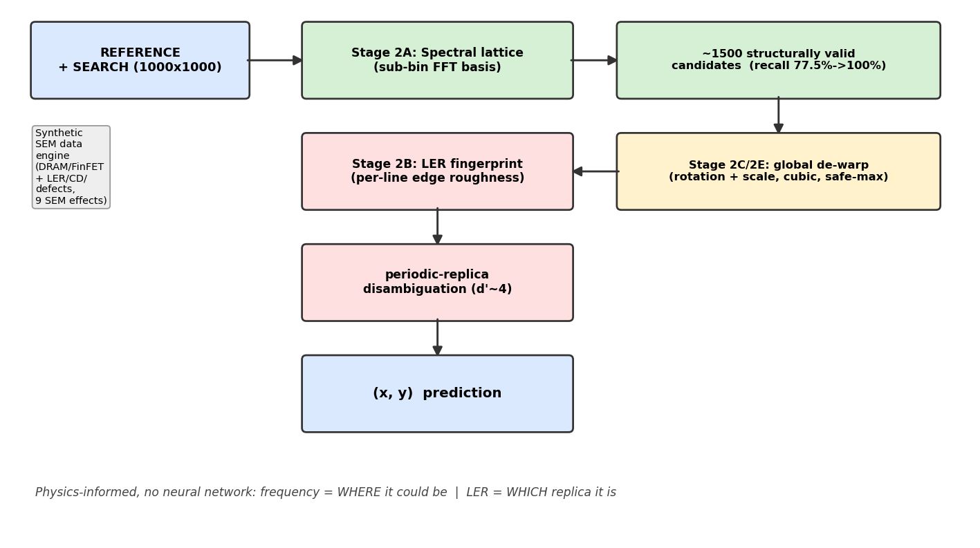
End-to-End Drift-Sense Localization Pipeline
-
Periodic Ambiguity: Why Classical Matching Fails
-
100% Alias Failure on Periodic Structures
-
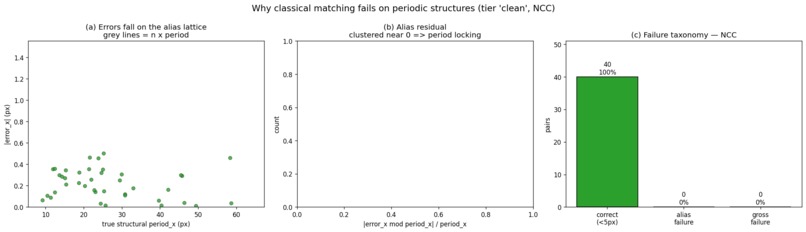
Clean Structures: Classical Matching Baseline
-
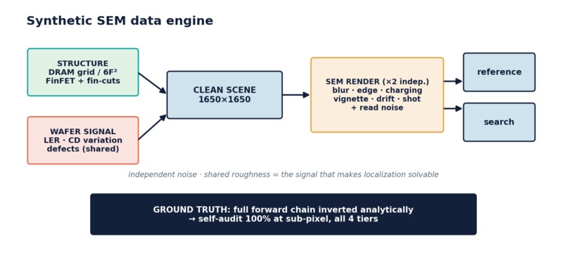
Physics-Based Synthetic SEM Data Generation
-
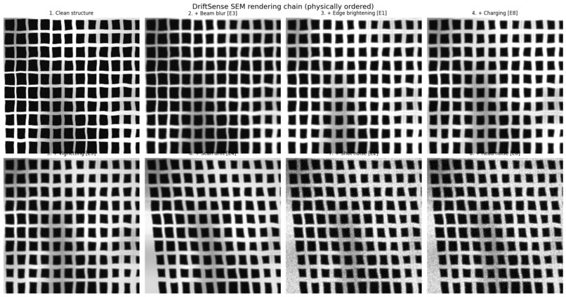
Physically Ordered SEM Imaging Effects
-
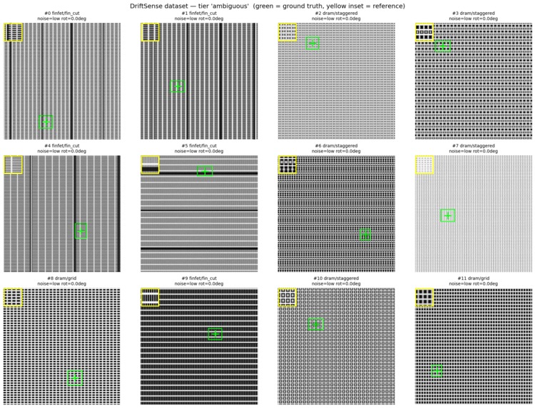
Ambiguous-Tier Dataset Diversity
-
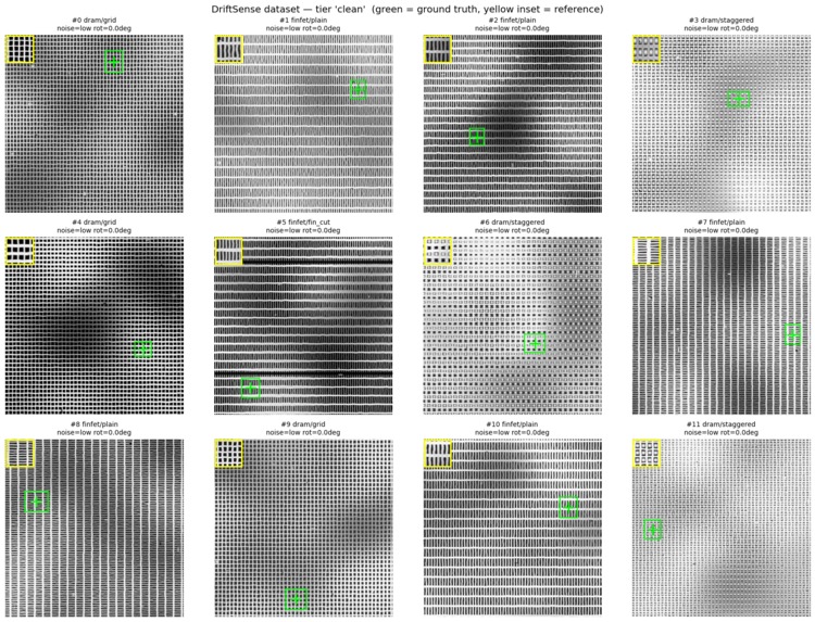
Clean-Tier Dataset Diversity
-
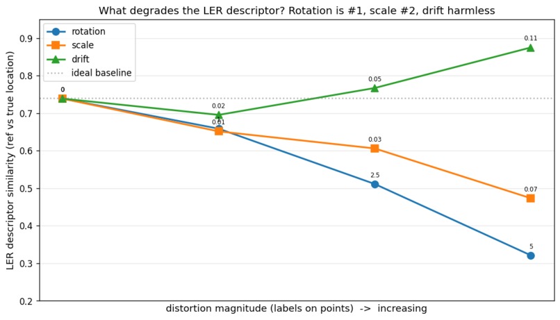
LER Descriptor Robustness to Distortion
-
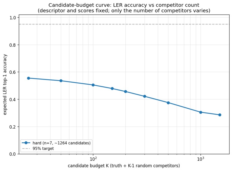
Candidate Reduction vs. LER Identification Accuracy

Inspiration
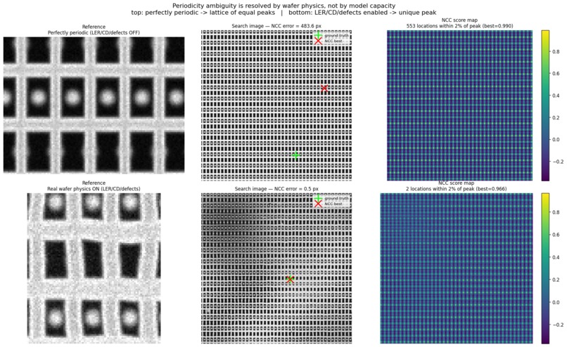
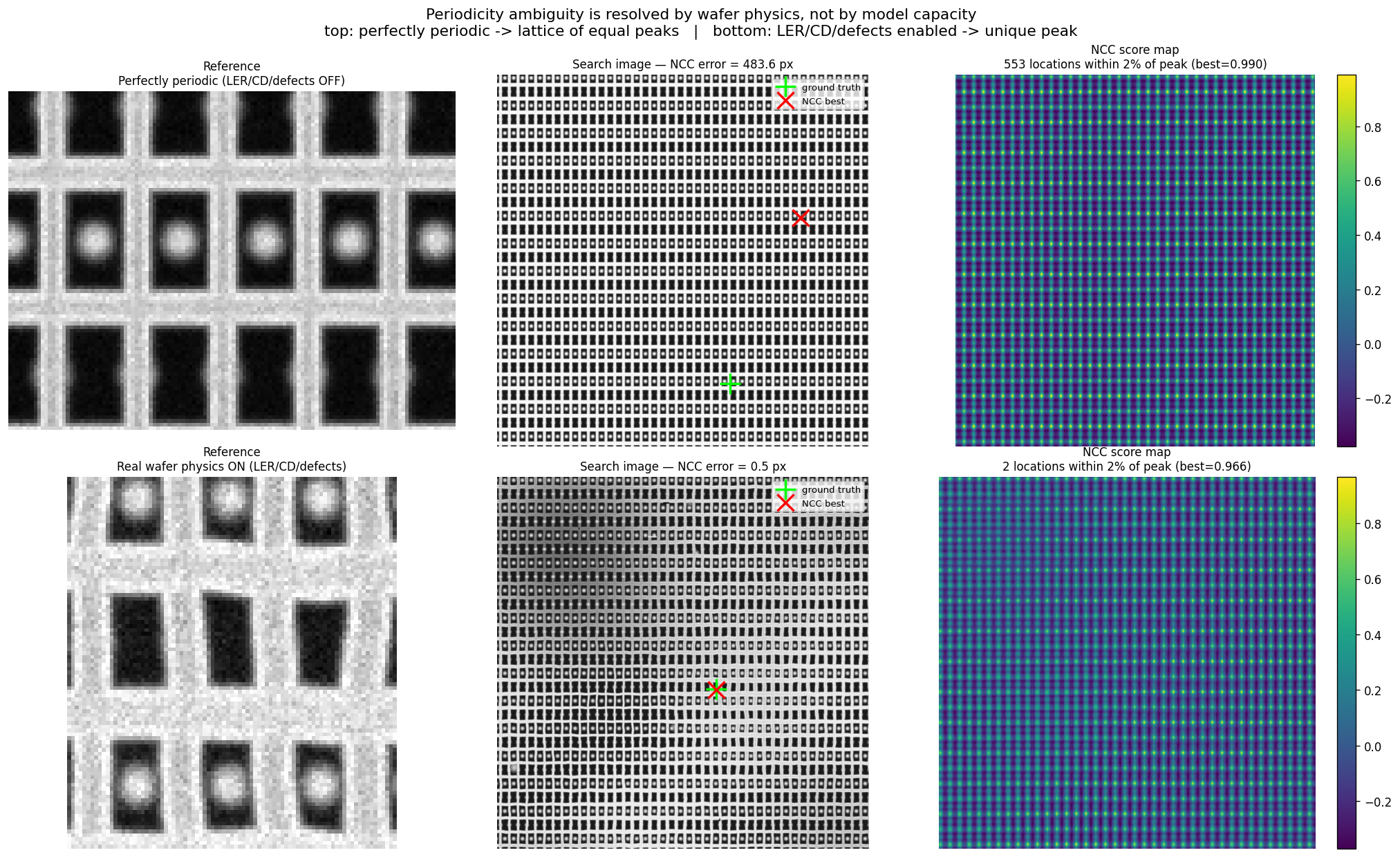
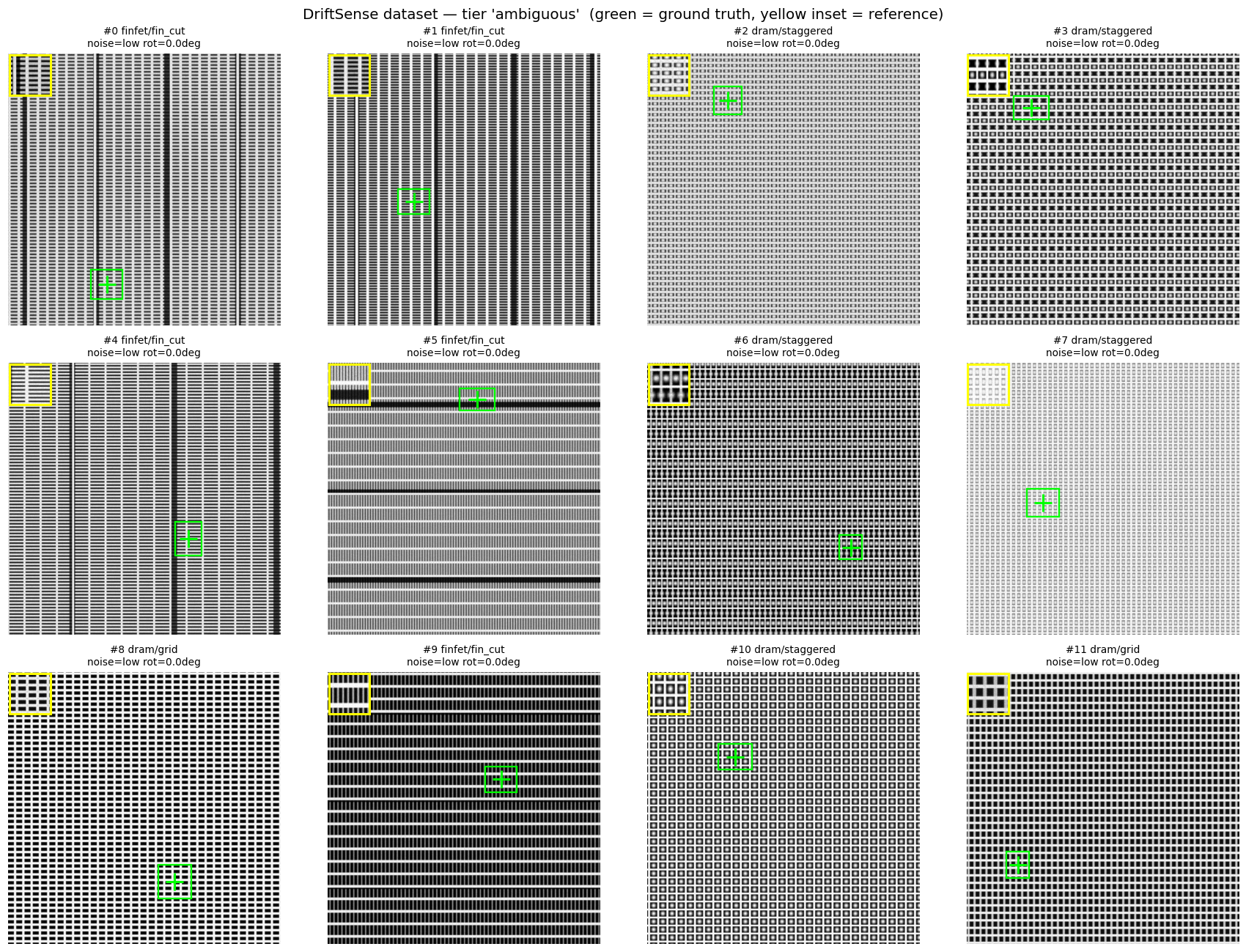
Semiconductor inspection images contain highly repetitive structures such as DRAM and FinFET patterns. This creates a fundamental localization problem: conventional template matching can lock onto a visually similar periodic replica instead of the true location.
While developing the project, we found that this failure was not simply a limitation of model capacity. In a perfectly periodic scene, multiple locations are genuinely indistinguishable. Real wafers, however, contain persistent physical variations such as line-edge roughness (LER), CD variation and defects. These imperfections can act as a physical fingerprint of a location.
This led to the central idea behind DriftSense: use the wafer's physical signature, rather than relying only on repeating geometric structure, to localize semiconductor inspection patterns.
What it does
DriftSense localizes a small reference SEM patch inside a 1000×1000 search image.
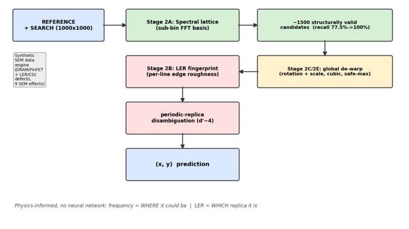
Instead of relying only on conventional normalized cross-correlation (NCC), the system uses a multi-stage approach:
- Candidate generation identifies structurally plausible locations using image and frequency-domain information.
- LER fingerprint extraction captures fine-scale, position-specific edge variations.
- Fingerprint matching re-ranks candidate locations using the physical signature of the wafer.
- Sub-pixel refinement estimates the final localization coordinate.
- Distortion handling accounts for rotation, scale and scan-related effects.
The key insight is that periodic structure determines where a pattern could occur, while persistent wafer-specific roughness provides information about where it actually occurs.
How we built it
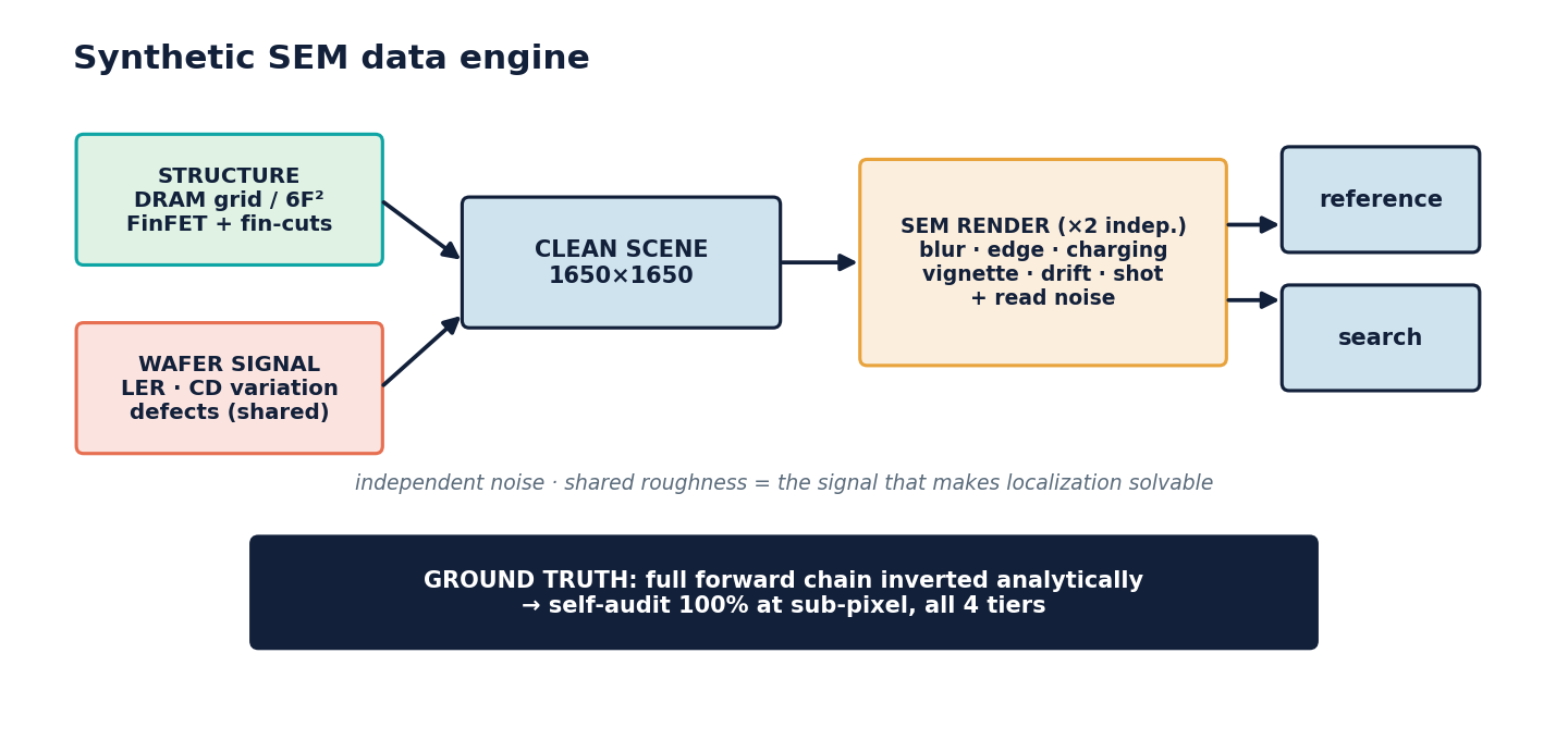
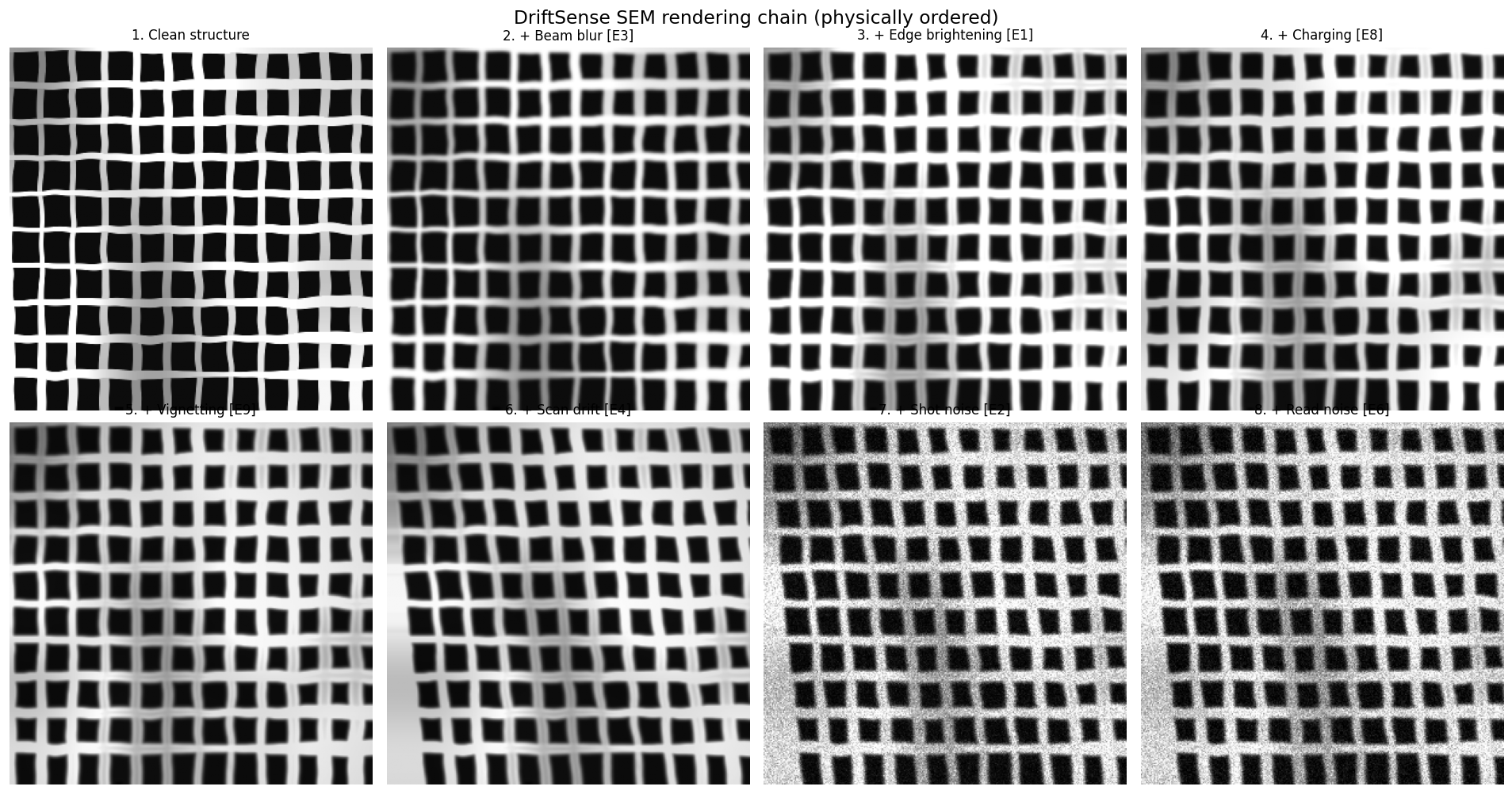
We first developed a physics-based synthetic SEM data engine covering DRAM and FinFET structures. The generator models line-edge roughness, CD variation, contrast drift, defects and a sequence of SEM acquisition effects including beam blur, edge brightening, charging, vignetting, scan drift, photometric response, gain jitter, shot noise and detector read noise.
The localization pipeline was then developed incrementally:
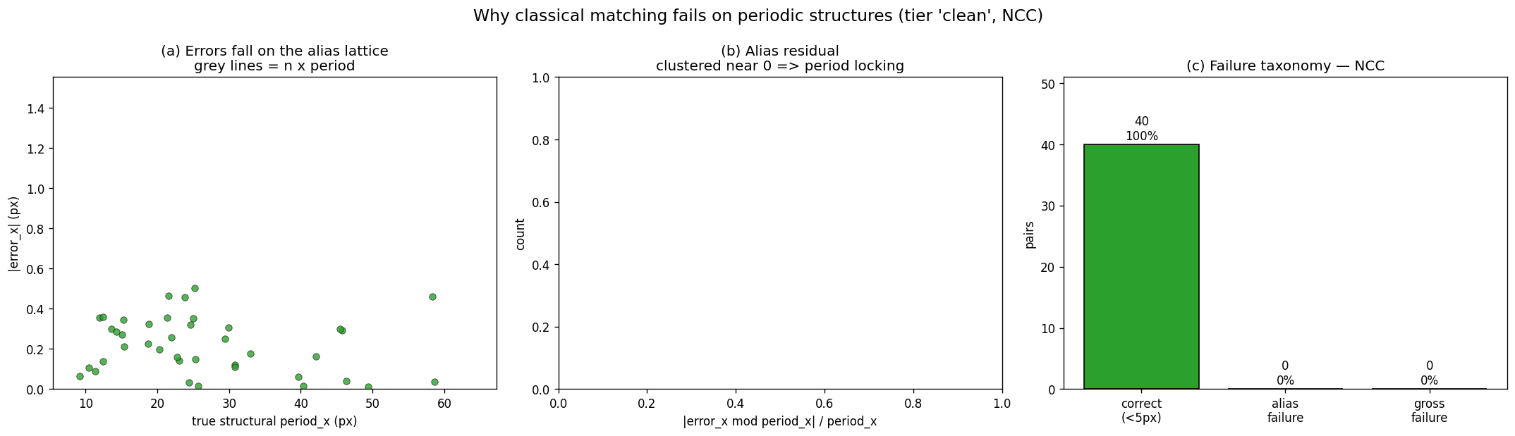
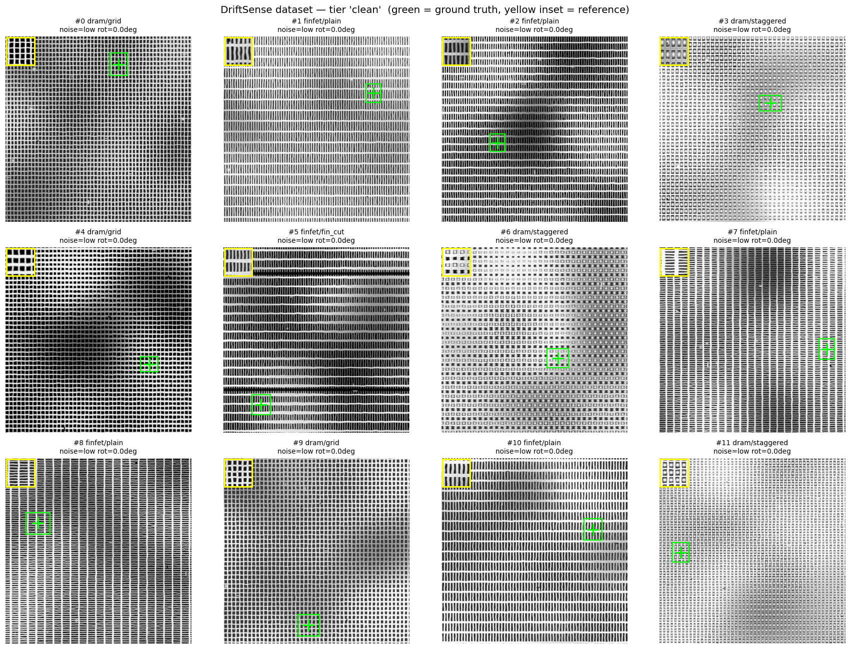
- A classical NCC baseline was established.
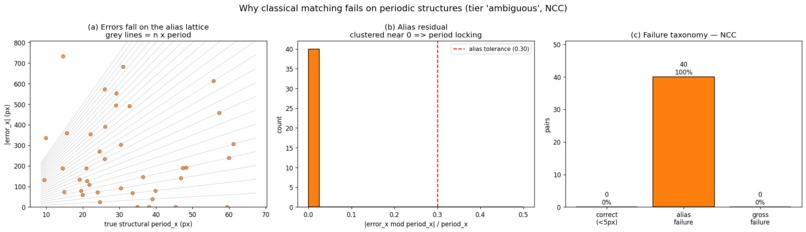
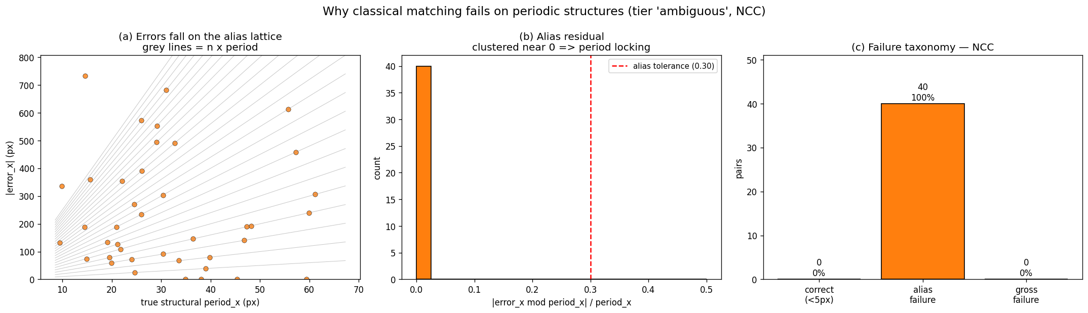
- Controlled experiments were used to identify periodic aliasing as the dominant failure mode.
- A LER fingerprint extractor was developed to exploit persistent wafer-specific roughness.
- Spectral analysis was added to generate lattice-constrained candidates and improve recall.
- Rotation and scale compensation were investigated through frequency-domain estimation and controlled experiments.
- A safe de-warp strategy was introduced so that geometric correction could improve a candidate without causing regression when its estimated transform is unreliable.
The system also includes automated ground-truth auditing so that generated image pairs and their localization labels remain geometrically consistent.
Challenges we ran into
The largest challenge was distinguishing genuine algorithmic failures from failures caused by the experimental setup.
We discovered and corrected several issues during development, including incorrect line rendering, ground-truth errors under scan drift, border artifacts introduced during image warping, and an aliasing problem in the original validation procedure.
A second challenge was the periodic nature of semiconductor structures. A candidate can have an almost identical coarse structure to the correct location while being hundreds of pixels away. This made simply improving NCC insufficient.
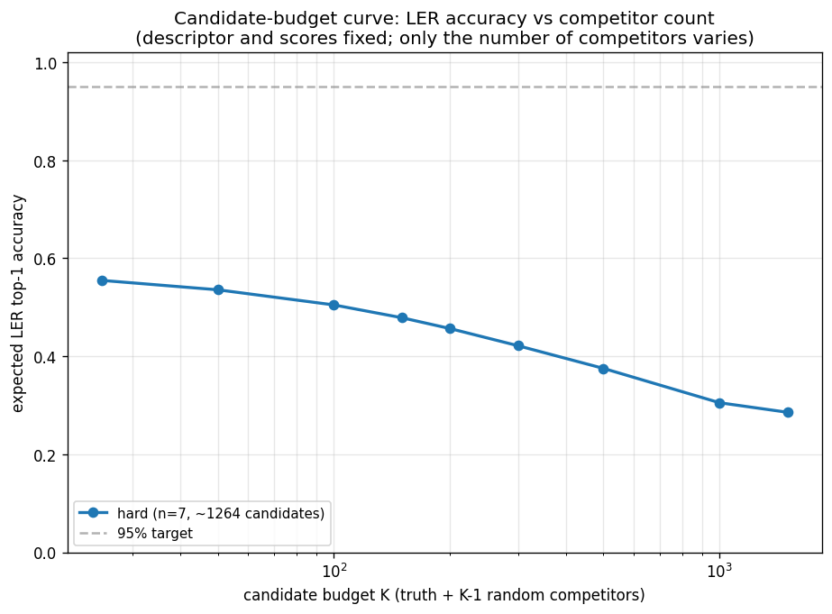
The next challenge was scaling the LER discriminator from a small number of periodic replicas to thousands of structurally valid candidates. Experiments showed that candidate-set size and descriptor robustness become critical as the number of competitors increases.
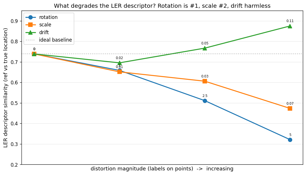
Finally, rotation and scale distortions affect the fine LER signal differently. We found that scale correction could be estimated accurately, while robust orientation estimation on highly periodic grids remained the main technical gap.
Accomplishments that we're proud of
The project produced several results that changed our understanding of the localization problem.
In controlled experiments, removing persistent wafer physics reduced LER-based discrimination to approximately chance, while enabling LER increased top-1 discrimination to 95–100%. The LER extractor recovered the injected roughness with a correlation of 0.997 under clean conditions.
Spectral candidate generation solved the candidate-recall problem on our hard synthetic set, improving lattice recall from 77.5% to 100% after sub-bin frequency refinement.
The system also demonstrated a measurable end-to-end improvement on difficult cases. With lattice candidates and LER matching, hard-tier accuracy improved from 10% with NCC to 40% in the reported 20-pair experiment.
Most importantly, the project established an information-theoretic control: when all persistent physical fingerprints are removed and the scene becomes perfectly periodic, localization falls to 0%, demonstrating that the system is exploiting physical information rather than artificially recovering unavailable positional information.
What we learned
Our biggest lesson was that the most important signal is not necessarily the largest visual feature.
The repeating semiconductor geometry is visually dominant, but it is also what creates ambiguity. The much smaller line-edge variations contain positional information because they are persistent properties of the physical wafer.
We also learned to treat controlled negative results as part of the engineering process. Several seemingly promising approaches failed: NCC-based ranking discarded the advantage of structural candidate generation, low-frequency prefilters removed the true location too often, and certain image resampling operations blurred the sub-pixel signal we were trying to measure.
These experiments helped us narrow the problem from "find a better matcher" to a more specific engineering challenge: build a distortion-robust, computationally efficient comparison of wafer-specific physical fingerprints.
What's next for DriftSense
The current system has established the physics-aware localization approach, but the next stage is focused on making it robust enough for broader evaluation.
Our primary technical goal is robust orientation estimation on periodic semiconductor grids. The current experiments show that oracle rotation and scale correction can substantially improve localization, while estimated orientation remains the main source of the remaining gap.
We also plan to complete the unified pipeline and evaluate it on the held-out test set that has been generated but not used for development.
Beyond the current synthetic environment, the longer-term direction is to validate whether persistent wafer-specific signatures can support practical SEM inspection and metrology workflows, where reliable localization can reduce ambiguity in highly repetitive semiconductor structures.

Log in or sign up for Devpost to join the conversation.