Inspiration
Hardware development is brutally slow. Getting from an idea to a manufactured prototype typically takes weeks of schematic capture, PCB layout, enclosure design, firmware development, and manufacturing file preparation - and that's if you already know how to do all of it. If you don't, you're hiring a hardware engineer and waiting months.
The obvious question is: can AI just do it? The answer has been "not reliably." LLMs hallucinate, and in hardware, one wrong connection means a dead board after manufacturing. You can't iterate on a PCB the way you iterate on code - each cycle costs real money and weeks of lead time.
Phaestus didn't appear from nowhere. It's the convergence of years of prior projects, each of which solved one piece of the puzzle:
CircuitSnips - My first attempt at a package manager for hardware subcircuits. Featured by Hackaday. TOKN - A 92% token reduction format for making KiCad files LLM-readable. Built because I wanted to see if LLMs could generate circuits, but discovered KiCad schematic files aren't optimised for it. KiDoom - DOOM rendered on KiCad PCB traces via a custom vector rendering engine. Hit #1 on Hacker News. Taught me programmatic PCB layout generation. OpenSCAD-DOOM - 3D DOOM running in a parametric CAD tool. Taught me programmatic 3D geometry generation.
CircuitSnips inspired the block catalogue. TOKN informed the constrained approach. KiDoom taught me to generate PCBs programmatically. OpenSCAD-DOOM taught me to generate enclosures. Phaestus puts them all together.
What it does
Phaestus is a web application that turns a plain English product description into everything you need to manufacture a real device. You describe what you want, and it produces:
- Specification - Gemini analyses feasibility, refines requirements, and produces a buildable spec
- PCB Design - Selects and places validated circuit blocks, merges schematics, generates Gerber files, BOM, and pick-and-place data
- Enclosure - Generates parametric OpenSCAD geometry with 3D preview
- Firmware - Generates source code and compiles it via cloud PlatformIO service
- Export - Packages all manufacturing files and supports browser-based device flashing
The key insight: instead of asking an LLM to invent circuits from scratch, Phaestus constrains the design space. It assembles products from pre-validated circuit blocks - human-designed, tested modules arranged on a standardised grid with defined bus interfaces. Think npm packages, but for hardware. The LLM's job shifts from "design a circuit" to "select and compose the right blocks." Outputs are correct by construction.
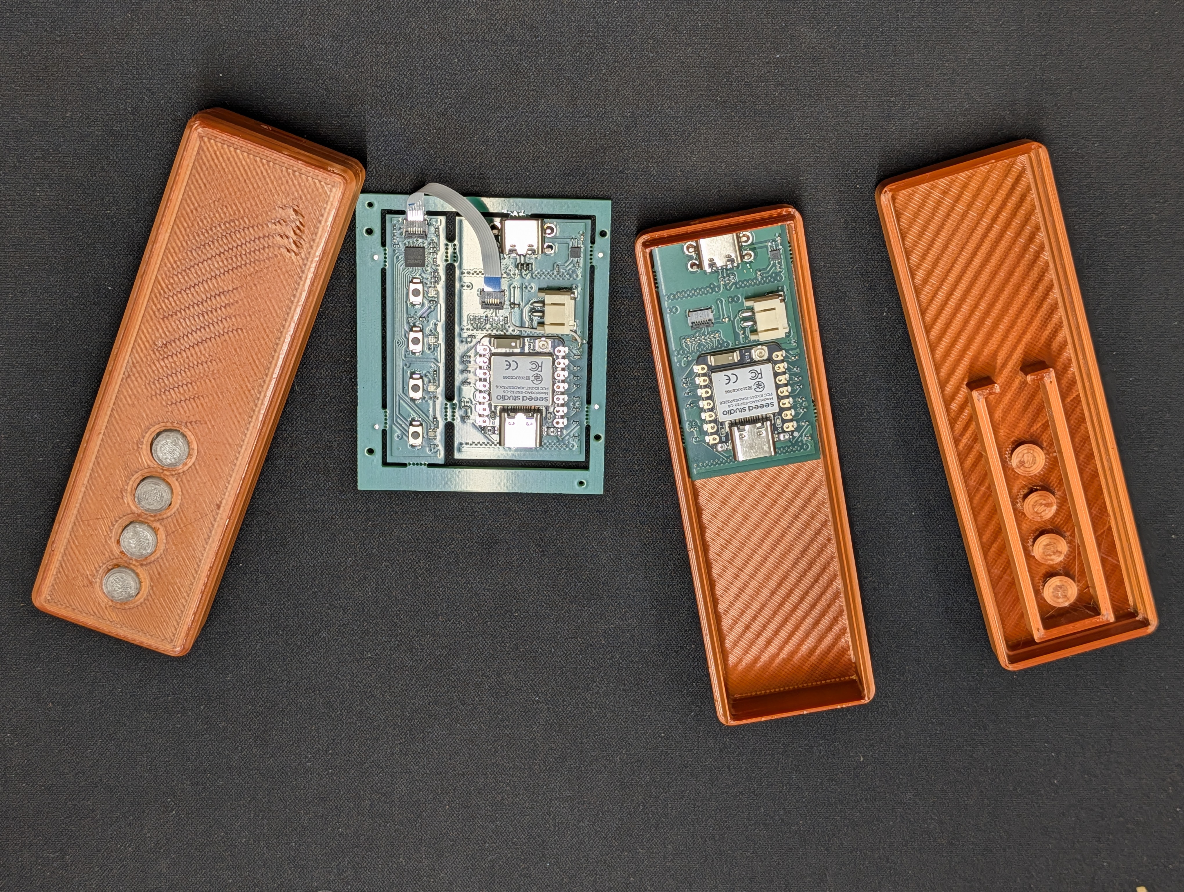
Proof it works: I described a Bluetooth remote control to Phaestus. In under five minutes, it generated the full design. I ordered the PCB assembled from JLCPCB, 3D-printed the enclosure, flashed the firmware from the browser - and it works. A real, manufactured product, designed by AI.
Gemini is the core intelligence behind every stage: feasibility analysis through multi-turn structured reasoning, block selection and composition against the catalogue, firmware generation tailored to the block configuration, parametric enclosure design, and blueprint image generation. The entire pipeline runs through LangGraph-based orchestration with all LLM responses parsed and validated against Zod schemas.
How we built it
Frontend: React 19 + TypeScript + Vite, with Tailwind CSS 4. Heavy client-side processing - manufacturing file operations (Gerber merging, BOM generation, PCB panelisation) run entirely in the browser.
Backend: Cloudflare Pages Functions - a thin serverless edge layer handling auth, persistence, and API key management. No persistent server.
Database & Storage: Cloudflare D1 (SQLite at the edge) for project data, R2 for object storage (design files, Gerbers, 3D models).
AI Orchestration: Google Gemini via the Gemini API, orchestrated through LangGraph with structured state graphs. All LLM responses parsed and validated with Zod schemas to ensure structured, reliable outputs at every stage.
Microservices: PlatformIO service for firmware compilation, KiCad service for PCB/schematic file generation. Both host-agnostic, connected via environment variables.
CI/CD: GitHub Actions deploying to Cloudflare Pages. Single command deploy.
The entire project was built evenings and weekends over approximately six weeks, solo, while maintaining a full-time job.
Challenges we ran into
Reliability over creativity: The hardest decision was choosing not to pursue unconstrained LLM circuit generation. It's the sexier approach, but it produces unreliable outputs. Constraining the design space to pre-validated blocks was the breakthrough - it turns an open-ended research problem into a tractable engineering problem. Manufacturing file fidelity: Gerber files, drill files, and pick-and-place data have to be pixel-perfect or the fabrication house rejects them. Getting browser-based Gerber merging to produce JLCPCB-compatible output required significant debugging. End-to-end integration: Each stage (spec, PCB, enclosure, firmware, export) has different file formats, different validation requirements, and different failure modes. Orchestrating them into a coherent pipeline that doesn't break on edge cases was the bulk of the engineering work. Cost management: Every generation has real API cost. Building on evenings and weekends while self-funding means being very deliberate about when and how to call the model.
Accomplishments that we're proud of
The manufactured Bluetooth remote control is the headline - a real, physical, working product designed by AI in under five minutes. Not a simulation, not a render, not a demo. A PCB manufactured and assembled by JLCPCB, a 3D-printed enclosure, firmware flashed from the browser. It works.
Beyond the demo piece, the full pipeline is working end-to-end: natural language in, manufacturing files out. Browser-based Gerber merging, cloud firmware compilation, and device flashing from the web app. The entire thing runs on Cloudflare's edge with no persistent server.
Building this solo, evenings and weekends, in roughly six weeks - while shipping production hardware at my day job - is something I'm proud of. The constrained block architecture means the approach scales: every new validated block expands what Phaestus can build without requiring the model to get smarter.
What we learned
The most important lesson: the right constraint is more valuable than a better model. By limiting the design space to pre-validated blocks, Phaestus sidesteps the hallucination problem entirely. The LLM doesn't need to be perfect at circuit design - it needs to be good at selection and composition, which is a much more tractable problem.
LangGraph with Zod schema validation turned out to be essential for reliability. Structured state management between pipeline stages means failures are catchable and debuggable rather than silently propagating bad data downstream.
Manufacturing is unforgiving. Software developers are used to fast iteration cycles - deploy, test, fix, redeploy. Hardware doesn't work that way. Every manufactured board costs money and takes days to arrive. This constraint shaped the entire architecture: validate everything before it leaves the browser.
What's next for Phaestus
- Expanding the validated block catalogue to cover more IoT use cases
- Adding a marketplace for community-contributed circuit blocks
- Direct integration with PCB fabrication houses for one-click ordering
- Support for more complex multi-board designs
- Opening access via a waitlist with usage credits
Built With
- cloudflare
- gemini
- gerber
- kicad
- kicanvas
- openrouter
- openscad
- platformio
- railway
- react
- tailwind
- three.js
- typescript
- vertex
- vite
- workos

Log in or sign up for Devpost to join the conversation.