-
-
UI
Inspiration
Imagine making the mistake of sending a board to JLCPCB and getting it back two weeks later only to realize the USB traces were the wrong impedance the whole time. You stare at it and think: I could have caught that in five minutes if I just did the math! Therefore, we wanted to build a tool that easily does the checking before the board leaves your computer, without running heavy professional software.
What it does
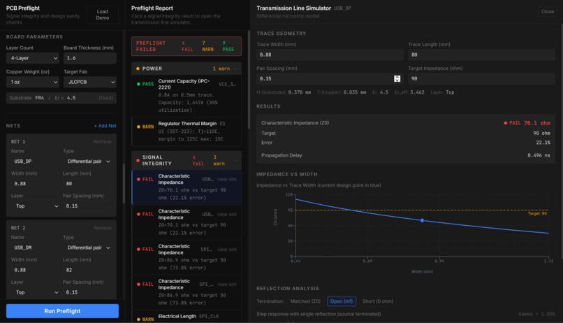
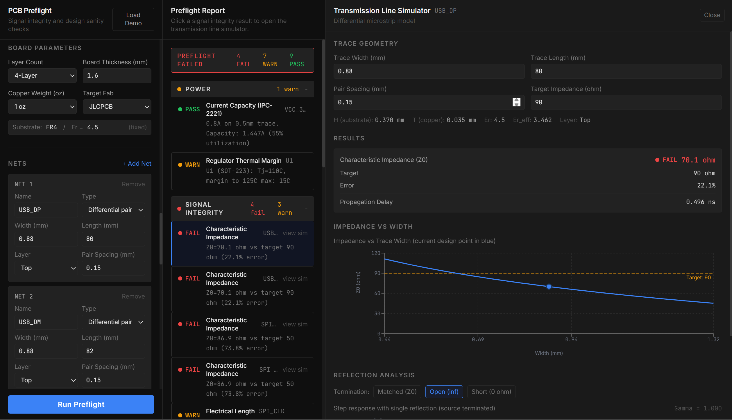
PCB Preflight takes your board parameters (layer stackup, trace geometry, components) and runs a set of engineering checks before you send anything to fab.
It checks characteristic impedance for microstrip and stripline traces using IPC-2141A models, flags differential pairs that are outside the USB 90 ohm or general 100 ohm targets, warns you when a trace is electrically long relative to the signal frequency, checks power trace current capacity against IPC-2221, computes junction temperatures for your regulators, and validates your geometry against the actual design rule minimums for JLCPCB, PCBWay, and OSH Park.
The centerpiece is the transmission line simulator that opens when you click any signal integrity result. It shows you a live impedance vs trace width curve, marks your current design point on it, and animates a step signal traveling down the line and reflecting back based on whichever termination you select. You can drag the inputs and watch the curve move.
It also parses real .kicad_pcb files. Drop your board file in, and it extracts nets, trace widths, trace lengths, layer assignments, and component footprints directly from the layout. Anything it can't determine from the file — current draw, power dissipation, thermal resistance — gets flagged clearly so you know exactly what to fill in before running checks.
How we built it
Pure frontend, no backend. React with Vite, Tailwind for styling, Recharts for the plots.
All the engineering math lives in a separate engineering/ directory with no React, isolated and independently testable.
The KiCad parser is a hand-written S-expression tokenizer and recursive descent parser. KiCad's file format is a nested Lisp-style tree and we didn't want to pull in a dependency for something that straightforward to implement. The parser handles quoted strings, numeric coercion, the version-dependent unit system, and differential pair detection from net name suffix patterns.
The demo board parameters were calculated backwards from the formulas to guarantee specific failure conditions, in order to provide a straightforward demo.
Challenges we ran into
The impedance formulas look simple on paper but have real geometric constraints. The IPC-2141A microstrip model breaks down at certain width-to-height ratios, so we had to think carefully about what the sweep plot would show at the edges of the range and make sure the calculator didn't produce nonsense values that would confuse users.
The KiCad parser had a few edge cases that took longer than expected. Footprint nodes can be arbitrarily deep and some properties we needed were nested several levels down. The unit normalization for older file versions also wasn't obvious from the format documentation. We had to test against actual exported files to confirm where the version cutoff was and what it affected.
Getting the differential pair detection right required a post-processing pass over all nets rather than per-segment classification, because you need to see all the net names before you can match pairs by base name and suffix. The ordering of that pass relative to power net classification also mattered since a net named VBUS_P could theoretically match both heuristics.
What we learned
The hardest part of an engineering tool isn't the math, it's deciding what to do when inputs are missing or out of range. Every check needed a clear policy on null inputs rather than silently producing wrong answers, and building that into the preflight runner as an explicit blocking step rather than a silent skip made the whole thing more trustworthy.
What's next for PCB Preflight
- Gerber file support so the tool works for other PCB files too.
- A stackup editor so you can define custom layer configurations rather than relying on the standard 2-layer and 4-layer approximations
Built With
- javascript
- react
- recharts
- tailwindcss
- vite


Log in or sign up for Devpost to join the conversation.