-
-
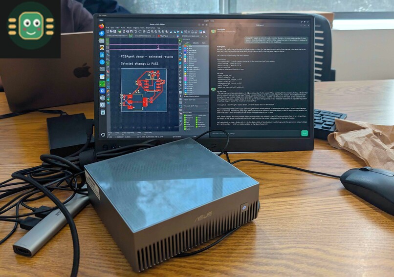
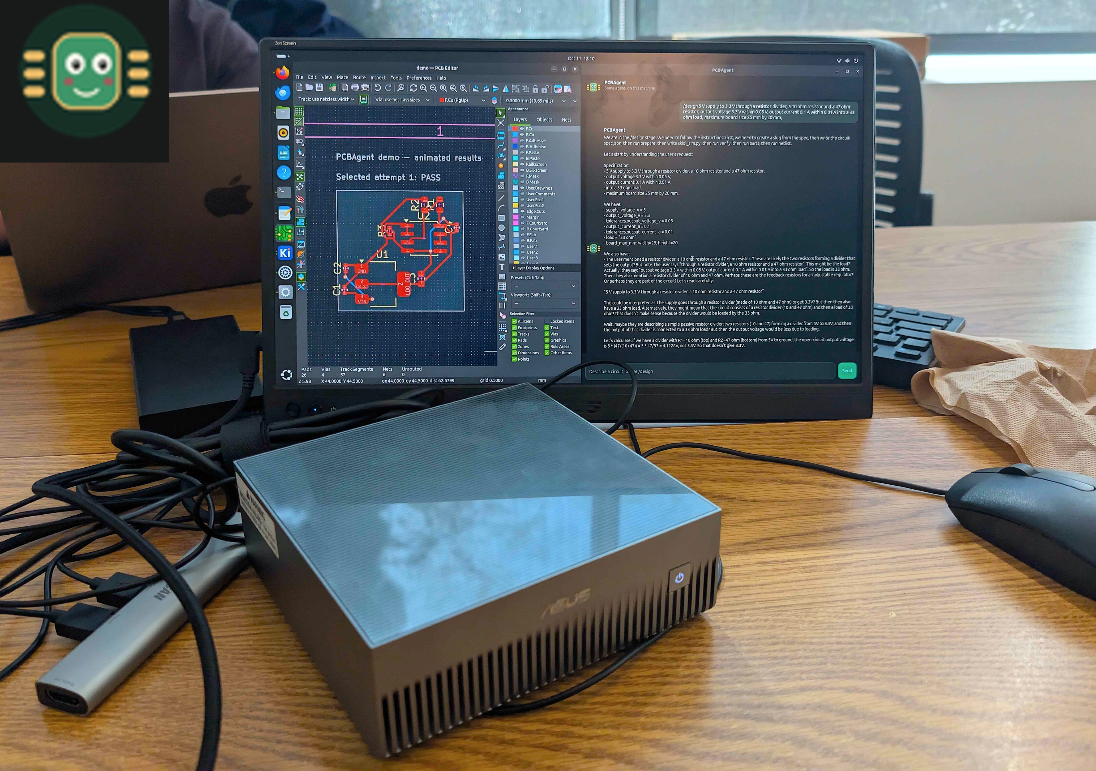
ASUS GX10 demo
-
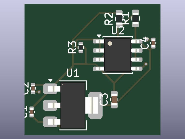
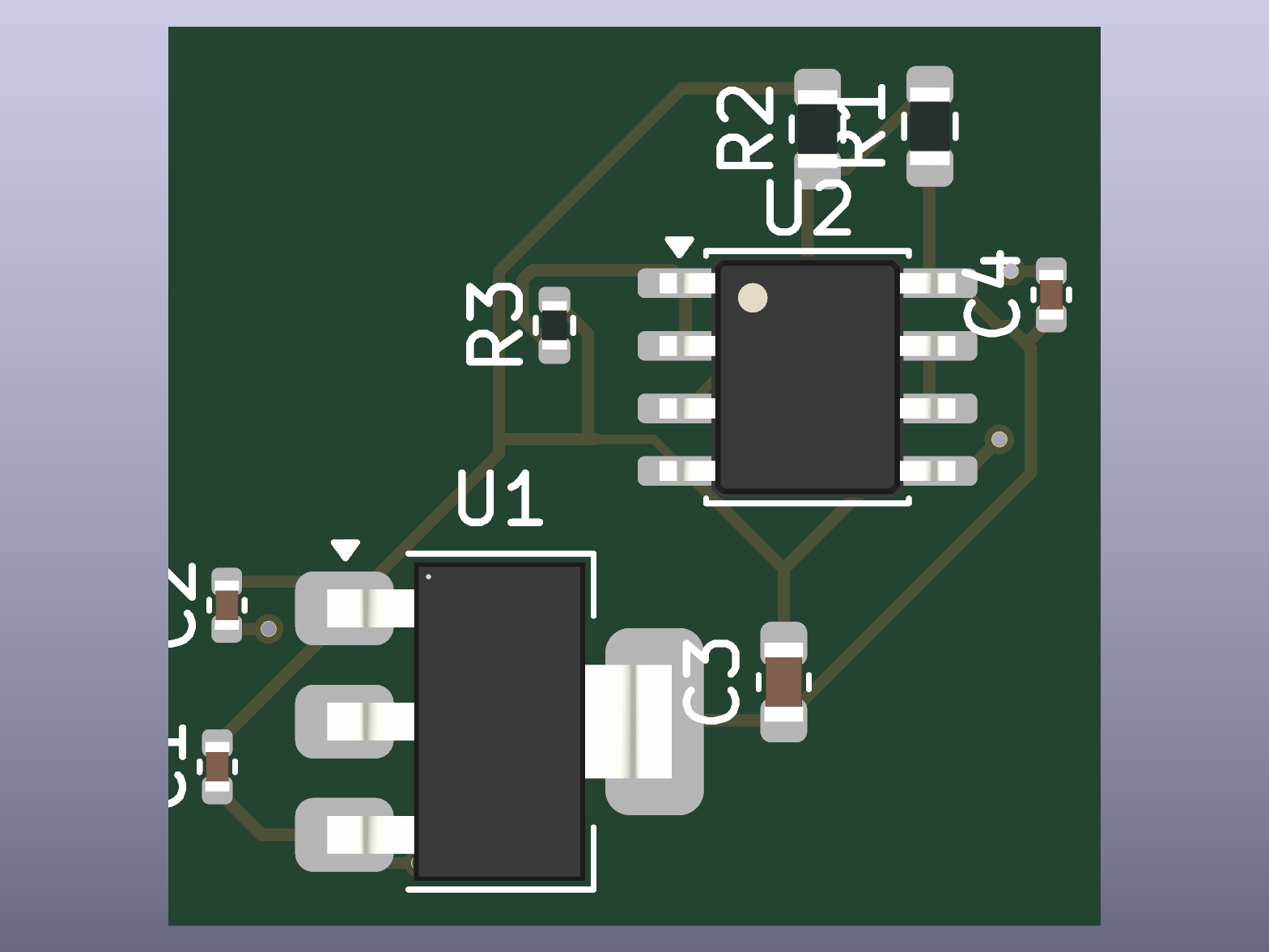
LDO Op Amp Board
-
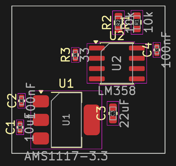
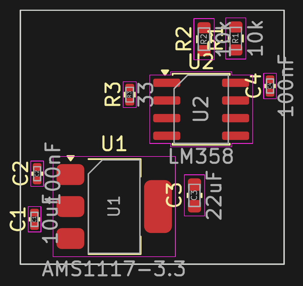
LDO Op Amp Placement
-
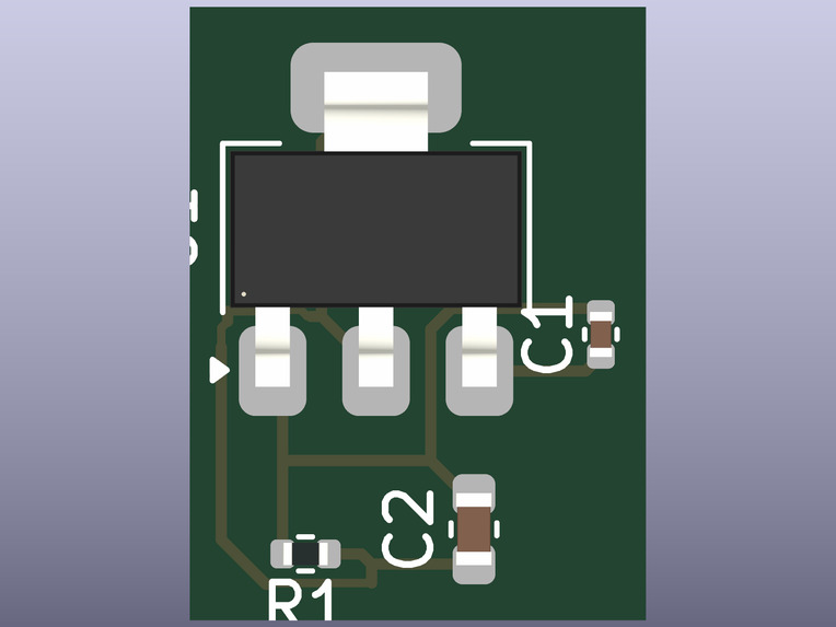
LDO Board
-
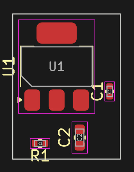
LDO Placement
Inspiration
PCB design is slow, tedious, boring work. Even small decisions, such as what part to use, whether a circuit actually behaves as expected, where components should go, and how traces should be routed require real electrical engineering expertise. While EDA tools like KiCad give engineers a powerful set of tools, these workflows still leave most of the grunt work to the person using them. There are existing AI-powered PCB design solutions, such as Flux AI, but these come with serious privacy and security concerns. For hardware design teams, schematics contain the core intellectual property (IP) of the product itself. Moving proprietary designs to the cloud introduces severe risks of information leaks, such as revealing circuit topology, unique component combinations, custom interfaces, or constraint strategies before a product ever hits the market. In highly competitive industries, a single data breach or third-party server vulnerability could compromise a company’s entire hardware portfolio. By executing the entire design lifecycle completely locally, hardware teams can maintain absolute control over their design security. A local architecture creates an air-gapped environment where sensitive design details remain strictly confidential, allowing companies to innovate rapidly without worrying about data sovereignty or cloud-based intellectual property exposure. We introduce PCBAgent, an agent that accepts a circuit specification in natural language, and can generate a circuit, test it against the original requirements, revise it when verification fails, and work through a full placement routing of PCB layout. Our work creates an automated, verified, and manufacturable PCB without requiring the design or the proprietary netlist to ever leave the user's machine.
What it does
One request becomes a checked board. The model writes the circuit. SPICE, the parts catalog, the placer, and KiCad decide whether that circuit is true. After the first prompt, the run continues on its own until you cancel it, and you can watch placement and routing in KiCad while it does.
Specify and simulate. /design writes a circuit spec and a SKiDL file. SKiDL emits a SPICE netlist, and ngspice runs it. The model does not hand-write a simulator deck.
Verify. Each acceptance number in the spec, such as output voltage and current, is compared with the ngspice measurement inside the stated tolerance. A value counts only when that simulation produced it. A miss stays inside /design: the model changes the circuit and the same checks run again. It does not edit the spec to hide a failure.
Select parts and write the netlist. Passives and the regulator are matched to a local JLCPCB catalog. Stock, price, and footprint names are copied from that cache and from the installed KiCad libraries. The same connections become a KiCad netlist with those symbols and footprints.
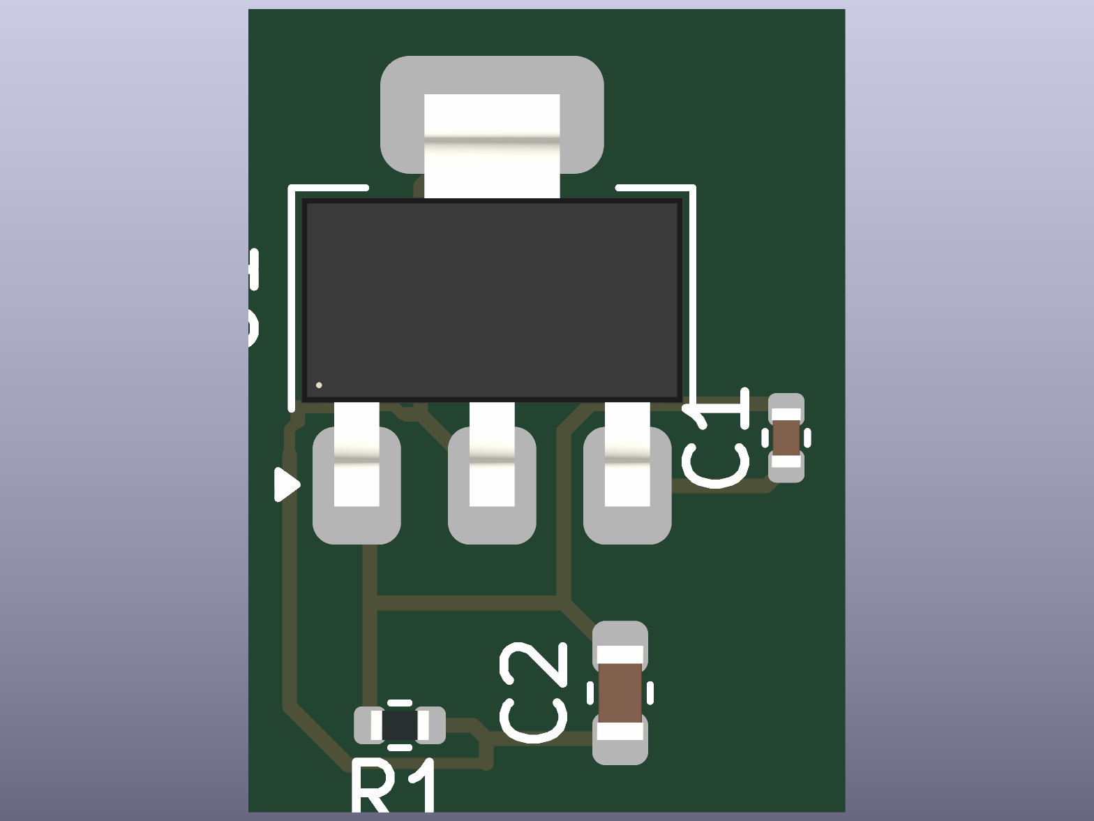
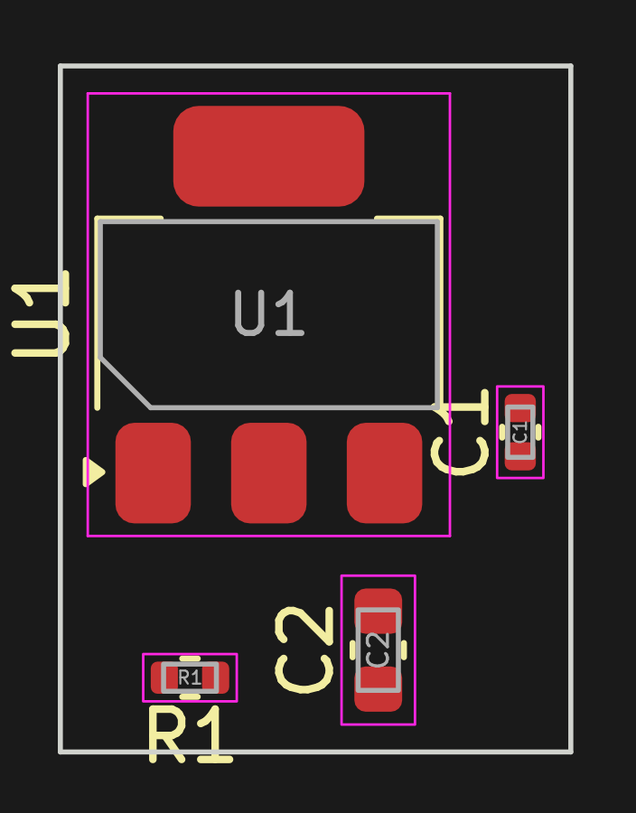
Place and route. /layout asks the model for placement constraints, such as a capacitor next to its IC. It does not emit coordinates or traces. A placer chooses positions, Freerouting draws the copper, and KiCad's design-rule check scores the board. layout.py --demo records that sequence and plays it in the PCB editor with no further prompts.
How we built it
The agent is a Pi package. Nemotron runs locally through Ollama and writes the spec and the constraints. Python runners do the repeatable work: ngspice, the parts cache, KiCad, and Freerouting.
Challenges we ran into
Switching regulators sent the model into long repair loops, and one failure was a SKiDL library bug rather than the circuit. The tools themselves finish in seconds. We learned to demo a divider and an LDO, and to let the model choose while the tools prove the result.
Accomplishments that we're proud of
A simple sentence input becomes a board that has been simulated, sourced, and routed, all on the GX10. ngspice will not accept a copied target voltage. The parts come from a local JLCPCB catalog, not from the model. Placement and routing are done by tools, and KiCad's design-rule check scores the result. A 5 V to 3.3 V divider and an AMS1117 low-dropout regulator both passed that path, and the finished board plays back in the PCB Editor.
What we learned
The model can choose, and the tools should prove it. ngspice, the parts lookup, and the autorouter finish in seconds. The long waits were Nemotron rewriting a circuit it could not debug, including one failure that was a SKiDL library bug rather than the schematic. A switching regulator is the wrong demo. A divider and an LDO finish, and they make the ultimate case for local AI: the netlist, component selections, and routing strategies never leave the machine. Running inference locally guarantees that your user IP is inherently protected from day one. It proves that engineers don't have to choose between advanced AI automation and rigorous enterprise design security.
What's next for PCBAgent
Export gerbers, a drill file, a bill of materials, and a pick-and-place file from the routed board. Improve efficiency of inference by using more planned-out tool calling.
Built With
- asus-ascent-gx10
- freerouting
- jlcpcb
- kicad
- ngspice
- nvidia-grace-blackwell
- nvidia-nemotron
- ollama
- pi
- pytest
- python
- skidl


Log in or sign up for Devpost to join the conversation.