-
-
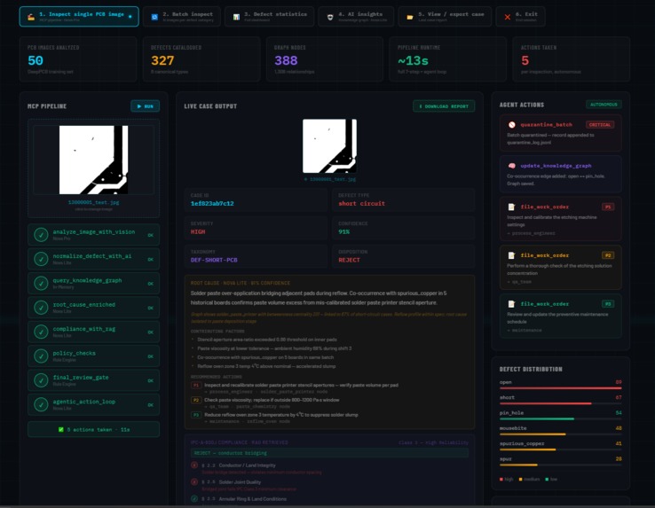
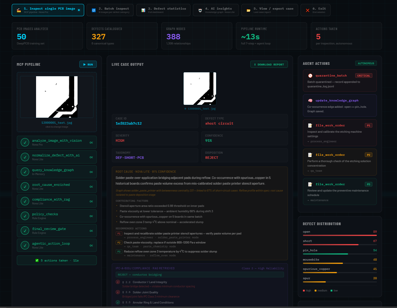
Live PCB inspection where Amazon Nova detects defects, checks compliance, finds root cause, and triggers actions automatically.
-
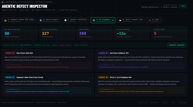
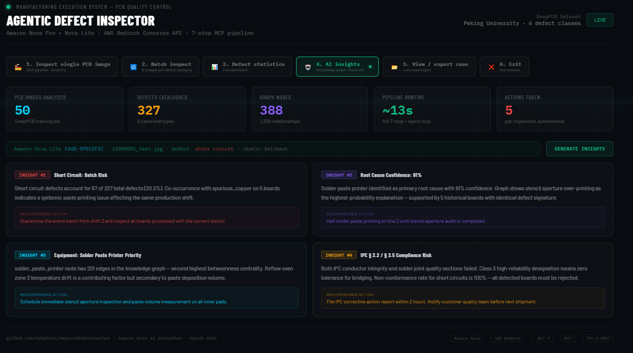
Knowledge graph insights highlighting defect trends, root-cause confidence, equipment risk, and IPC actions.
Inspiration
In manufacturing, failure rarely arrives with a warning. It starts as something small: a break in copper, a tiny hole, a subtle defect on a PCB that looks easy to miss. But if that defect slips through inspection, it can travel downstream into assembly, trigger rework, delay shipments, or become a field failure.
That was the problem that inspired this project. Most AI demos can describe what they see, but they stop there. They generate a caption, produce a report, and leave the real decision-making to a human. In a factory, that delay is expensive.
I wanted to build something more urgent and more useful: a system that does not just see a defect, but understands its manufacturing impact, checks whether it violates standards, and immediately helps drive the next action.
The problem
The core problem is not just defect detection. It is the time gap between detection and response.
A defective PCB should not wait in a queue for someone to read a report, interpret the issue, check compliance documents, decide severity, notify the right team, and create follow-up actions manually. By the time that happens, the board may already be too far along in the process.
There is another challenge too: raw image datasets are not enough on their own. We used the open-source PCBData dataset to train and evaluate defect understanding, but the dataset only gives the visual evidence. It does not tell the full operational story:
- what likely caused the defect
- what equipment might be involved
- whether the board should be accepted or rejected
- what the factory should do next
That missing layer between image and action is the real problem this project tries to solve.
Dataset used
We used the open-source PCBData dataset, based on real PCB defect imagery, as the visual foundation for the project. It gave us labeled examples of PCB defects such as open circuits, shorts, mousebites, spurs, pin holes, and spurious copper.
PCBData was critical because it gave us realistic defect images to inspect, but it also exposed the limitation of vision-only systems: even when a defect is visible, operational decisions still require reasoning, context, and standards knowledge.
What we built
Manufacturing Vision Analyzer is an agentic AI system for PCB defect inspection built on Amazon Bedrock with Amazon Nova.
The system analyzes PCB images, identifies the likely defect, normalizes it into a manufacturing-friendly taxonomy, queries a knowledge graph for related history and equipment context, checks IPC compliance, and then triggers actions such as quarantine logging, work-order generation, and knowledge graph updates.
In other words, it moves from: $$ \text{Image} \rightarrow \text{Defect} \rightarrow \text{Reasoning} \rightarrow \text{Action} $$
That last step is what makes the project different. This is not only an inspection demo. It is an operational response system.
How we built it
We built the project as a .NET 9 application with a multi-step AI pipeline.
Amazon Nova Pro handles the multimodal image analysis step. Amazon Nova Lite handles reasoning-heavy stages such as defect normalization, root-cause analysis, IPC compliance checks, and the final agentic loop. We used the Bedrock Converse API so the model could work with structured tools and return actionable outputs instead of only plain text.
To ground the system, we connected the model to a manufacturing knowledge graph built from PCB defect data and enriched it with defect relationships, historical patterns, equipment associations, and IPC references. We also added validation, policy checks, and review gates so the system does not act blindly.
Challenges we faced
The hardest challenge was turning vision into trustworthy action.
Detecting a defect is one thing. Deciding what to do about it is much harder. We had to make sure the model was not just persuasive, but structured and reliable. That meant defining tool schemas carefully, validating outputs, grounding decisions with standards and graph context, and making sure every action could be traced.
Another challenge came from the dataset itself. PCBData is powerful as an open-source foundation, but it does not come with business context, compliance decisions, or manufacturing workflow logic. We had to build that missing bridge ourselves. The images showed us what was wrong, but the system had to learn how to connect that defect to cause, severity, standards, and remediation.
We also had to balance capability and cost. Using the strongest model everywhere would be wasteful, so we split the workload between Nova Pro for vision and Nova Lite for reasoning and agentic actions.
What we learned
We learned that the real value of industrial AI is not in describing a problem. It is in reducing the time between discovering a problem and doing something about it.
We also learned that open-source datasets like PCBData are an excellent starting point, but not the full answer. In manufacturing, images alone are not enough. Real value comes from combining vision, domain knowledge, standards, and automation.
Most importantly, we learned that a defect report is only the beginning. What matters is whether the system can respond before the defect becomes a real-world failure.
Built With
- .net-9
- 99-x-26-for-the-built-in-we-have-to-add-what-languages
- amazon-bedrock
- amazon-nova-lite
- amazon-nova-pro
- apis
- aws-converse-api
- c#
- cloud-services
- databases
- deeppcb/pcbdata
- frameworks
- ipc-a-600j
- json
- knowledge-graphs
- model-context-protocol-(mcp)
- or-other-technologies-did-you-use?-can-you-do-it-with-the-commas>?-c#
- platforms
- react
- vite


Log in or sign up for Devpost to join the conversation.