-
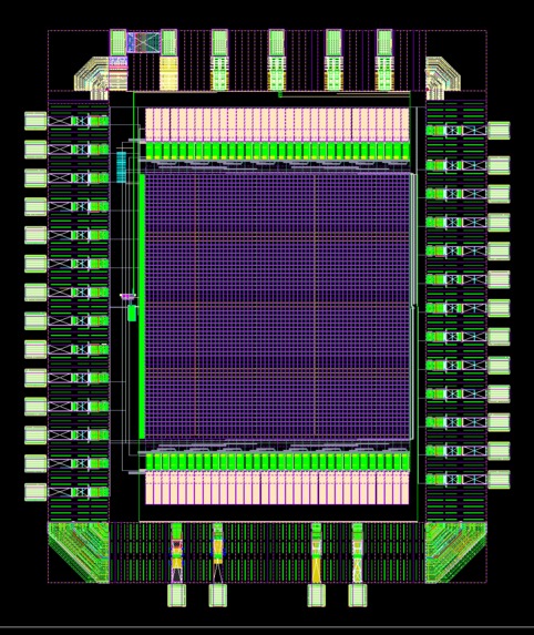
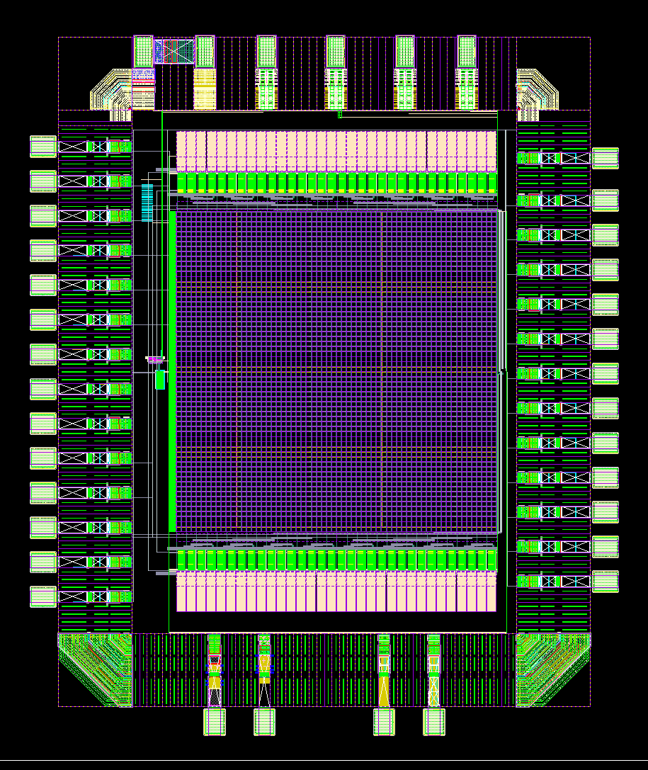
Final layout
-
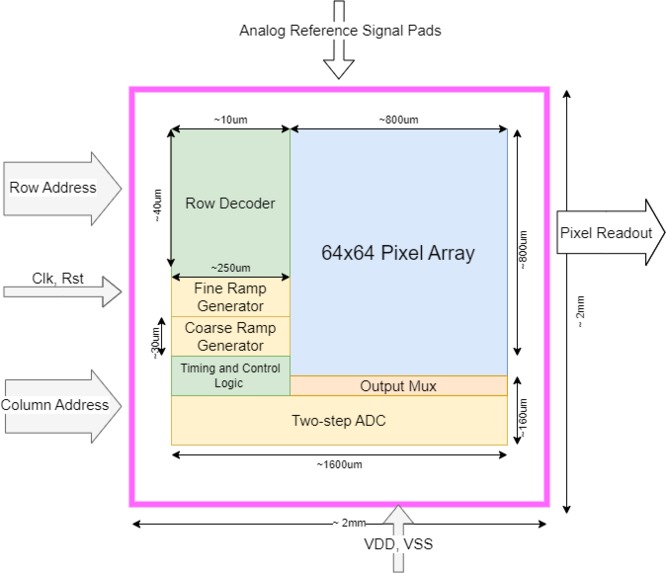
Top level system diagram.
-
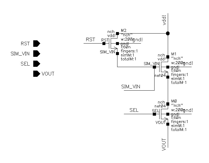
Single Pixel Schematic
-
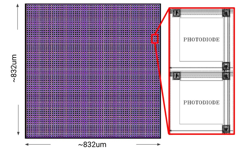
64x64 Pixels Layout
-
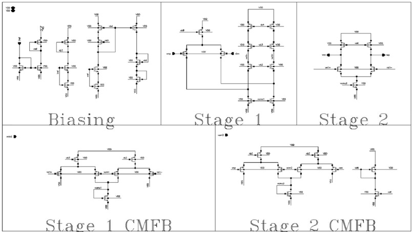
2-stage Subthreshold Amplifier Schematic
-
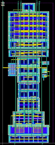
2-stage Subthreshold Amplifier Layout
-
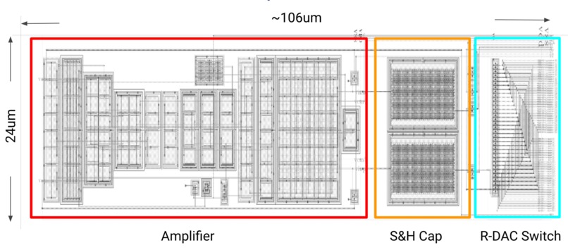
Two-step ADC Layout
-
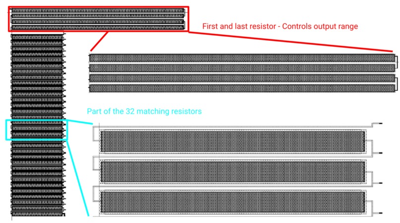
R-DAC layout
-
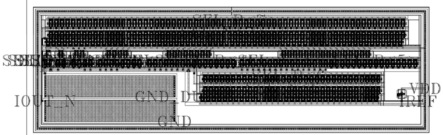
I-DAC Layout
-
Timing and Control Logic Layout
-
Row-Decoder Layout
Inspiration
This project is inspired by the paper "Low Power CMOS Image Sensors Using Two Step Single Slope ADC With Bandwidth-Limited Comparators & Voltage Range Extended Ramp Generator for Battery-Limited Application," by H. Park, C. Yu, H. Kim, Y. Roh and J. Burm.
What it does
This project presents the implementation of a low-power CMOS image sensor tailored for battery-constrained applications. The sensor captures 64×64 pixel images and digitally outputs the grayscale values of each pixel. Designed using the TSMC 65nm CMOS process with a 1.1V supply, it features a 2-step Single Slope ADC architecture, achieving 12-bit output resolution while consuming just 23μW of power per column.
The design integrates hand-drawn layouts for analog components (pixel sensor, ADC, DAC, ramp generator), alongside digital logics implemented through automated synthesis and place-and-route. The complete design has been integrated into a pad frame, passing LVS and DRC checks, and is ready for tape-out.
Top-Level Operation and System Specification
Refering to the picture titled "Top level system diagram".
- The design includes a 64x64 pixel array of 3 transistor (3T) pixel sensors
- The analog voltages collected from the pixel array are converted into 12-bits digital signals per pixel using the column 2-step ADC.
- The design can process one column of pixels at a time (64 pixels) using the column parallel two-step ADC.
- The resulting digital reading can then be read out pixel by pixel by controlling the row and column decoders, the row and column address are both provided externally through the input pads. The column ADCs share the two global ramp generators used for the 2-step operation.
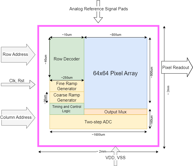
Top level system diagram
Components
Three-transistor Pixel Sensor
The 3 transistors (3T) pixel sensor includes 3 transistors and one photodiode, one transistor acts as the reset switch that charges the photodiode to VDD on a reset, one transistor acts as a source follower amplifier that converts the charge on the photodiode into a voltage signal, and another transistor acts as a switch to output the voltage. The voltage output reflects the amount of light that the photodiode is exposed to. A 9um x 9um space has been left out for the photodiode that was not implemented.
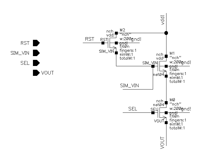
Single Pixel Schematic
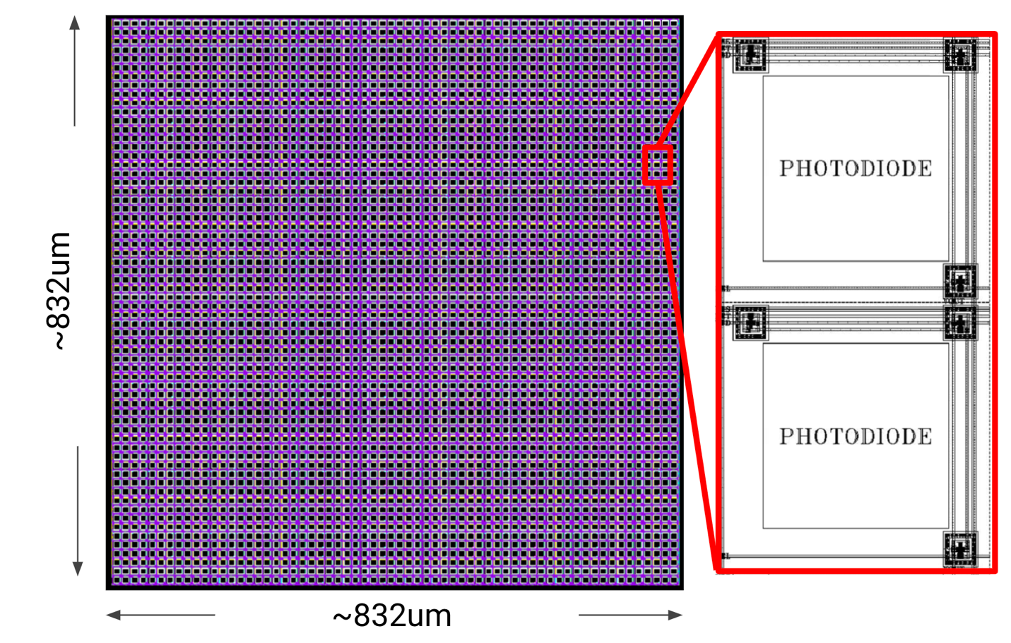
64x64 Pixels Layout
Two-step Analog to Digital Converter
The 2-step ADC makes use of a 2-stage subthreshold amplifier to achieve a gain of 76dB. The amplifier requires 100nA reference current and 650mV common mode voltage supplied externally through the analog pads.Full custom floorplan to minimize area, devices interdigitated and symmetrically routed for matching, and power grid is used to distribute power/ground evenly to mitigate electromigration and voltage drops.
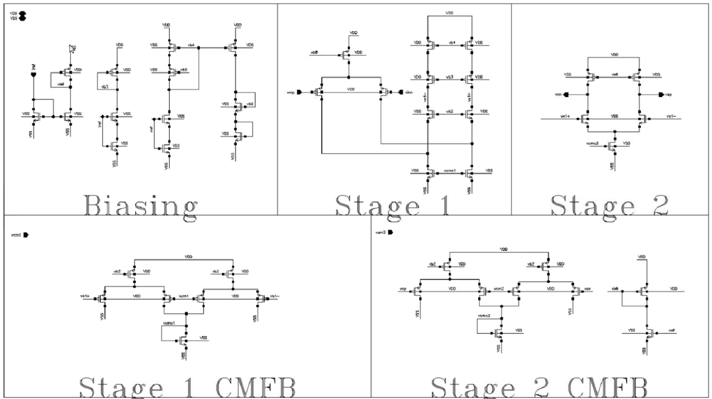
2-Stage Subthreshold Amplifier Schematic
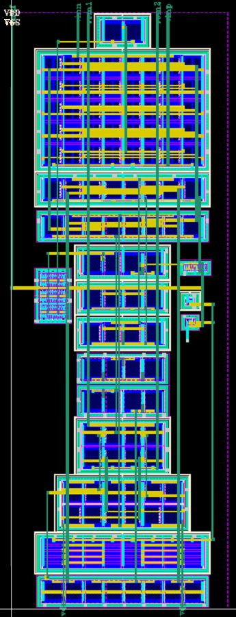
2-Stage Subthreshold Amplifier Layout
The ADC also requires sample and hold capacitors (S&H cap shown in figures) and resistor-DAC switches to operate. The complete schematic and layout of the 2-step ADC is shown below:
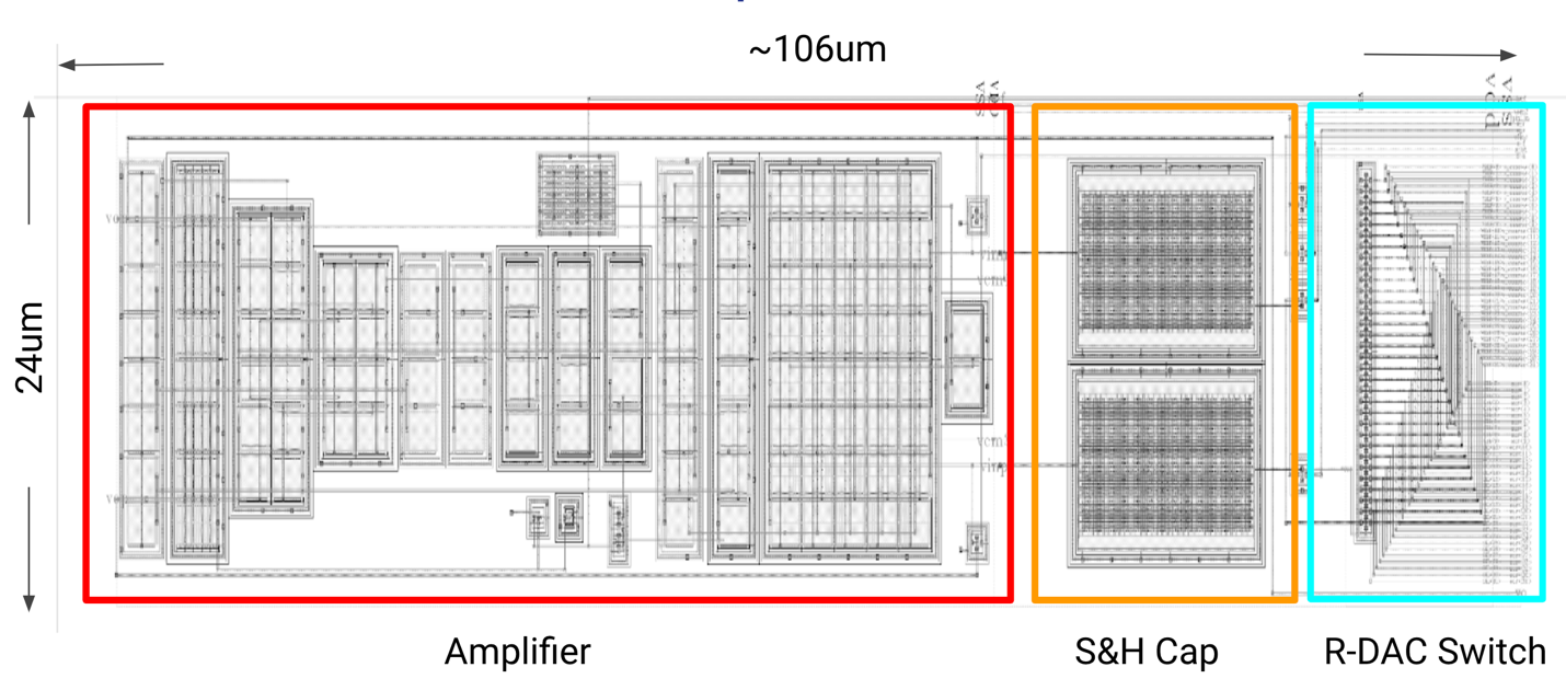
2-step ADC Layout
Ramp Generators
Coarse Ramp Generator (R-DAC)
The coarse ramp generator is a resistor ladder DAC that divides the output voltage into 32 stages using 32 matching resistors. The first and last resistor are sized to control ramp range. The output of the coarse ramp generator is fed into the coarse step of the 2-step ADC for reference voltage.
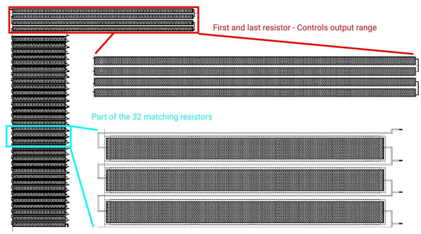
R-DAC Layout
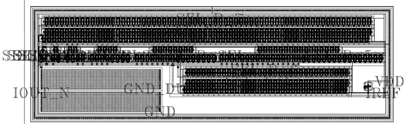
Fine Ramp Generator (I-DAC)
The fine ramp generator is a binary weighted current steering DAC (I-DAC). The differential switches are used to improve power and reduce dynamic errors and identical resistors are used to convert current to voltages.
R-DAC Layout
Timeing and Control Logic
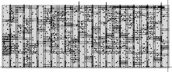
The timing and control logics is a digital block written in Verilog. It is synthesized then placed and routed using Innovus. This module is a sequential circuit that overlooks the entire pixel read out process. It features a finite state machine that decides the state of the operation and controls the R-DAC switches in the 2-step ADC. It also contains 2 counters that controls the output generation process for both the coarse and fine ramp generators.
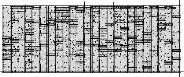
Timing and Control Logic Layout
6-bit Row Decoder
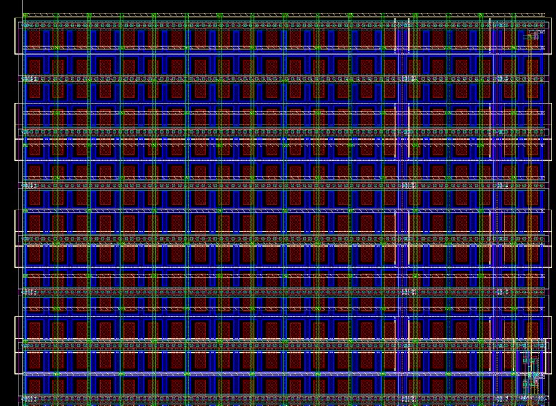
The 6-bits row decoder chooses one row of pixels out of the 64 available rows to output to the output pads. It is a digital block written in Verilog, synthesized then placed-and-routed using Innovus. The layout for this module is shown in figure 16. Note that this module is sized to match the height of the pixel array for easier routing (18um*832um), it is hard to include the entire layout in one picture, therefore, only a portion of the layout containing the output for a single row is shown.
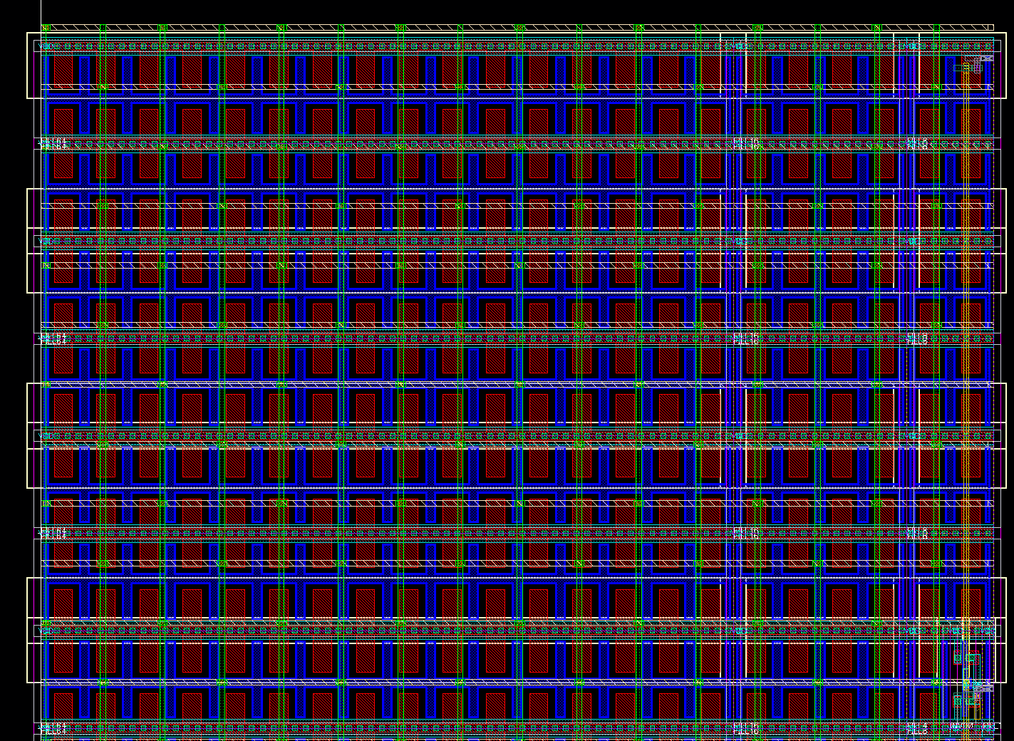
Row Decoder Layout
Built With
- innovus
- verilog
- virtuoso

Log in or sign up for Devpost to join the conversation.