
Executive Summary
CPUs, being scalar processors, are very slow at specialized, data-parallel computation. Many kinds of silicon chips will have specialized hardware for signal processing, video compression, machine learning, and other computationally expensive tasks. However, custom silicon chips (ASCICs) are extremely expensive and slow to design, verify, and manufacture. Moreover, they cannot be revised once fabricated. FPGAs (field programmable gate arrays), on the other hand, can implement arbitrary digital circuits, but also come with the advantage of being reconfigurable after fabrication. An FPGA chip has switching and interconnect for all the logic on the chip such that wired connections can be rerouted electronically. Somewhat similar to ASIC design, designing for FPGAs is currently extremely slow for large designs. This makes testing changes and debugging designs much more time consuming and mentally taxing than developing software. Furthermore, FPGA design often requires lots of expertise in all the idiosyncrasies of the target hardware and software toolchain. The problem we are attempting to tackle with our project is both the time commitment and expertise required to design FPGA-based accelerators.
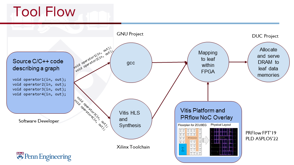
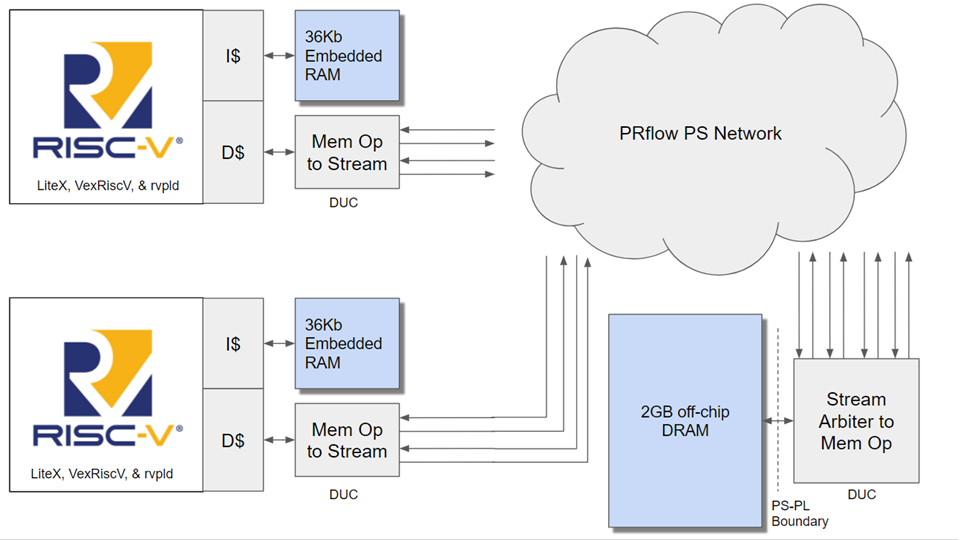
We present DUC: Data Unlimited Compile. By leveraging off-fabric DRAM, we can provide several orders of magnitude more memory capacity to the streaming operators within an accelerator. Our project is a framework that will enable FPGA developers to perform hardware-software integration testing, explore more design points quicker, and allow software engineers to utilize hardware software co-design without new training. There are ongoing efforts on a multitude of fronts that each tackle one aspect of design space exploration limitations. One such contribution is PRflow by Xiao which breaks down a monolithic HLS design into a separate compilation of building blocks. Still, the limitation remains that embedded memory residing on FPGA fabric is very limited. For example, the Ultra96 in the Zynq Ultrascale+ family has less than 1MB of on-fabric RAM but 2GB off-fabric. We hope to alleviate this design limitation by allowing the 2GB DRAM to be networked to any region of the FPGA floorplan using the existing overlay architecture of PRflow. Hence, this approach adds no additional FPGA resources or time in order to compile a design. By providing FPGA regions with an always-on option to use the substantially larger DRAM, the data memory footprints of HLS designs goes from being one of the largest constraints to having in a practical sense “unlimited” headroom.
Built With
- c
- hls
- verilog

Log in or sign up for Devpost to join the conversation.