-
-

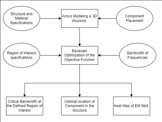
Block diagram
-

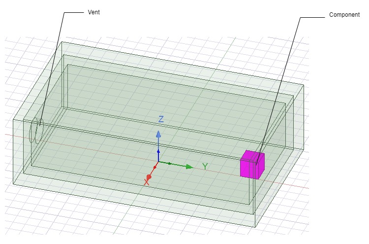
Simulation in progress
Inspiration
The advancement in the fields of AI and VLSI, alongside the penetration of Wireless technology and accessible Internet, has led to a rapid rise in the Consumer Electronics market. As per a recent report [1], the Consumer Electronics Market size was valued at over USD 1 trillion in 2020 and is estimated to grow at a CAGR of more than 8% from 2021 to 2027. Consumer Electronics find their use-case in several domains, from Entertainment Systems to critical applications like Healthcare and Automotive. In general, these products must adhere to rigid standards and undergo several compliance tests, of which testing for Electromagnetic Interference and Electromagnetic Compliance (EMI/EMC) is the most crucial. Electronic devices (even without transmitters) emit electromagnetic radiation, just as a byproduct of switching currents and voltages inherent to electronic circuitry. Without limits to the amount of unintended electromagnetic radiation from electronic products, the electromagnetic spectrum could be adversely affected, and frequency bands reserved for radio transmission could become compromised [2]. In critical cases like Medical, EMI/EMC performance can mean the difference between life and death – hence performing extensive EMI/EMC testing is a necessity and cannot be substituted for. This process, although necessary, is expensive, inaccessible, repetitive, and power-hungry i.e., not sustainable. As the number and complexity of devices will increase the need for this testing will proportionally surge. With the goal to accelerate the process and promote sustainable practices in EMI/EMC testing, we designed a cross-functional simulation environment that aids in the process of physical EMI/EMC testing. For instance, while designing a Class-III medical device like an Insulin Pump – the body of the pump with the location of components can be imported into our environment and a detailed EMI/EMC analysis (at various frequency bandwidths) can be generated. This would also promote the use of sustainable materials – as the cost of testing them significantly drops. The key idea of this project is to reduce the dependency on EMI/EMC test centres by providing apriori information through our simulation environment.
What it does
Standard EMC testing procedures subject a device to electromagnetic radiation to check how it behaves under such conditions. The circuit for these devices is intricately designed to inhibit interference and shield radiation from the circuit. These are then rigorously evaluated for EMI/EMC in a controlled environment – which is an expensive process, thus discouraging many small-medium scale (non-critical) products to avoid this entirely. This in turn adds to the problem of stray EM radiations. Our simulation environment was designed to be more accessible, and easy and to introduce sustainability in the energy-intensive EMI/EMC testing process through early identification, and mitigation of potential design hazards in electronic subsystems through state-of-the-art simulation and visualization. The simulation environment can apply a bandwidth of frequencies to a user-defined 3D model of any material and can generate a report with a heatmap of EM field strengths, and can also determine likely frequencies at which the EMI/EMC test might fail for a certain component location.
How we built it
The simulation environment was developed with the following design requirements:
- Generality – The users can design (on Ansys) and import any of their designs and perform this analysis on their custom structures. The users can also choose the packaging material of the body and of the components from a pre-defined library or a custom material. This means the user can at any time introduce a new material for a component/body and do a feasibility study of its effect on the EM field.
- Flexibility – The users can choose the one-or-more regions-of-interest for analysis and have the choice of selecting the bandwidth of frequencies for which they want to evaluate the design.
- Sustainability and Reliability – The analysis algorithm is built using Bayesian Optimization. That is, given runtime constraints it’ll have an efficient and faster Design Space Exploration and a higher likeliness of reaching global optima within a finite number of iterations. This ensures reliable solutions are achieved with limited compute time and energy – efficient and reliable.
The simulation environment employs three software/tools: Ansys, Python and MATLAB. Structure and material specifications and component placement and generates a 3D model with Ansys. The 3D model is then fed into a MATLAB code which then performs the optimization. Finally, the algorithm outputs critical bandwidth; the range of frequencies at which the EM field strength will be above the safe threshold at the given point based on the optimized component location.
Challenges we ran into
- Algorithm occasionally failed to compute the EM field at certain points due to complex 3D structure.
- 3D modelling on Ansys due to lack of design background
- Unable to perform full-scale validation due to lack of computational resources
- No open-source literature available for EMC devices and methods
Accomplishments that we're proud of
- Successfully developed a working Proof-of-concept of our idea.
- Designed a sustainable solution that can be easily adopted into the industry.
- Tested our system for 3 different material compositions and observed promising results.
- Approached the problem by applying Design Thinking techniques.
- Interviewed an industry professional in the field of EMI/EMC testing to get real-world insights.
What we learned
- Association between device structure and Electromagnetic Compatibility
- Relation between material variability and EMC
- Device electromagnetic compatibility dependence on the bandwidth of frequencies
- Modeling structures with the Ansys tool
- Bayesian Optimization of the 3-dimensional objective function
- Visualization of results with MATLAB
- Ansys, Python scripting, and optimization in MATLAB
What's next for EMC-Squared
- Scale the algorithm to multiple vents and components
- Scale the algorithm for multiple points and form a region of interest
- Bombard the device with EM waves with varying strengths and modulation
- Work closely with the industry to add features that can further aid in the EMI/EMC test.
Built With
- ansys
- bayesian-optimization
- machine-learning
- matlab
- python


Log in or sign up for Devpost to join the conversation.