-
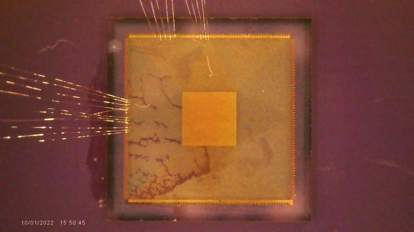
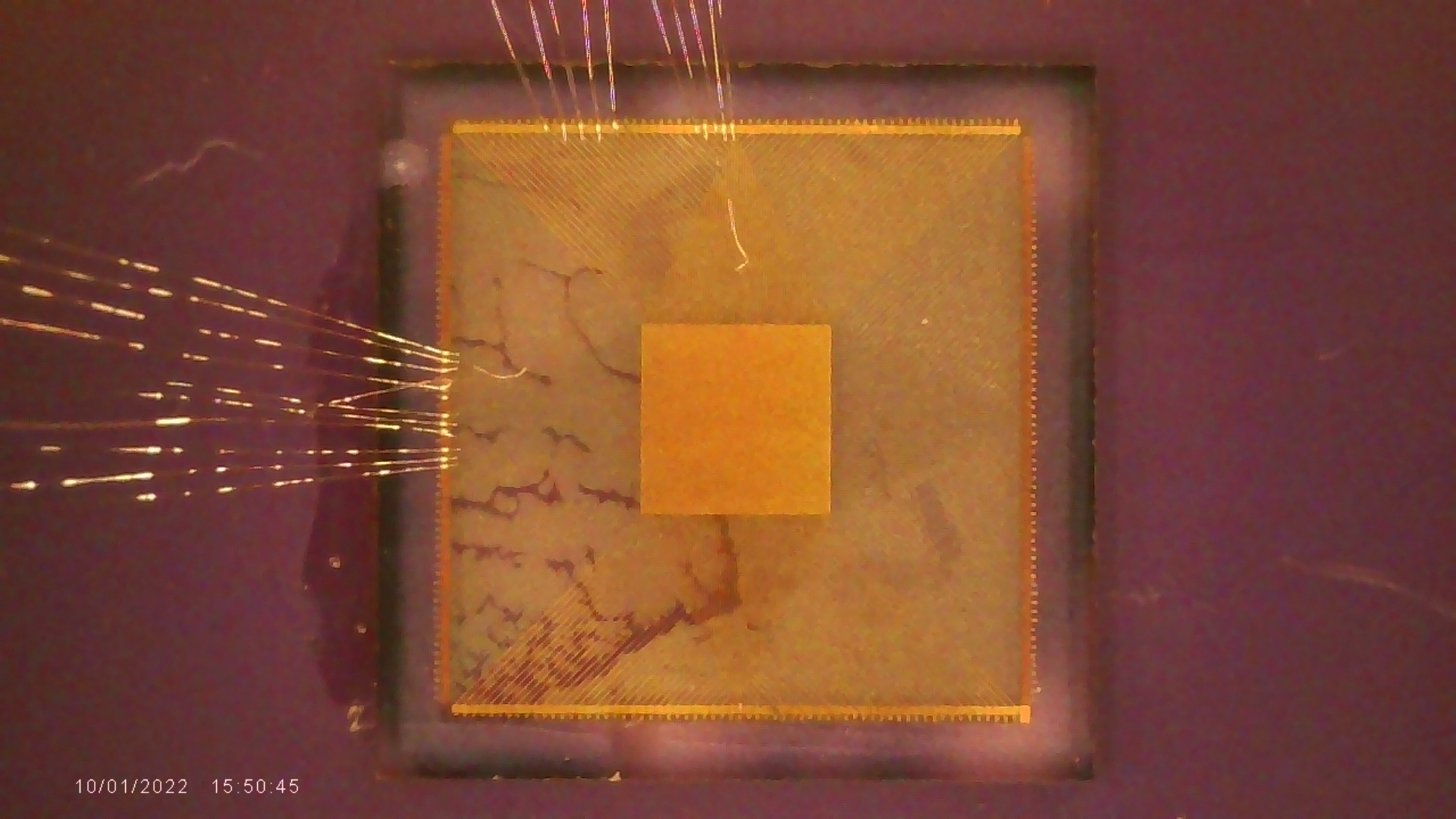
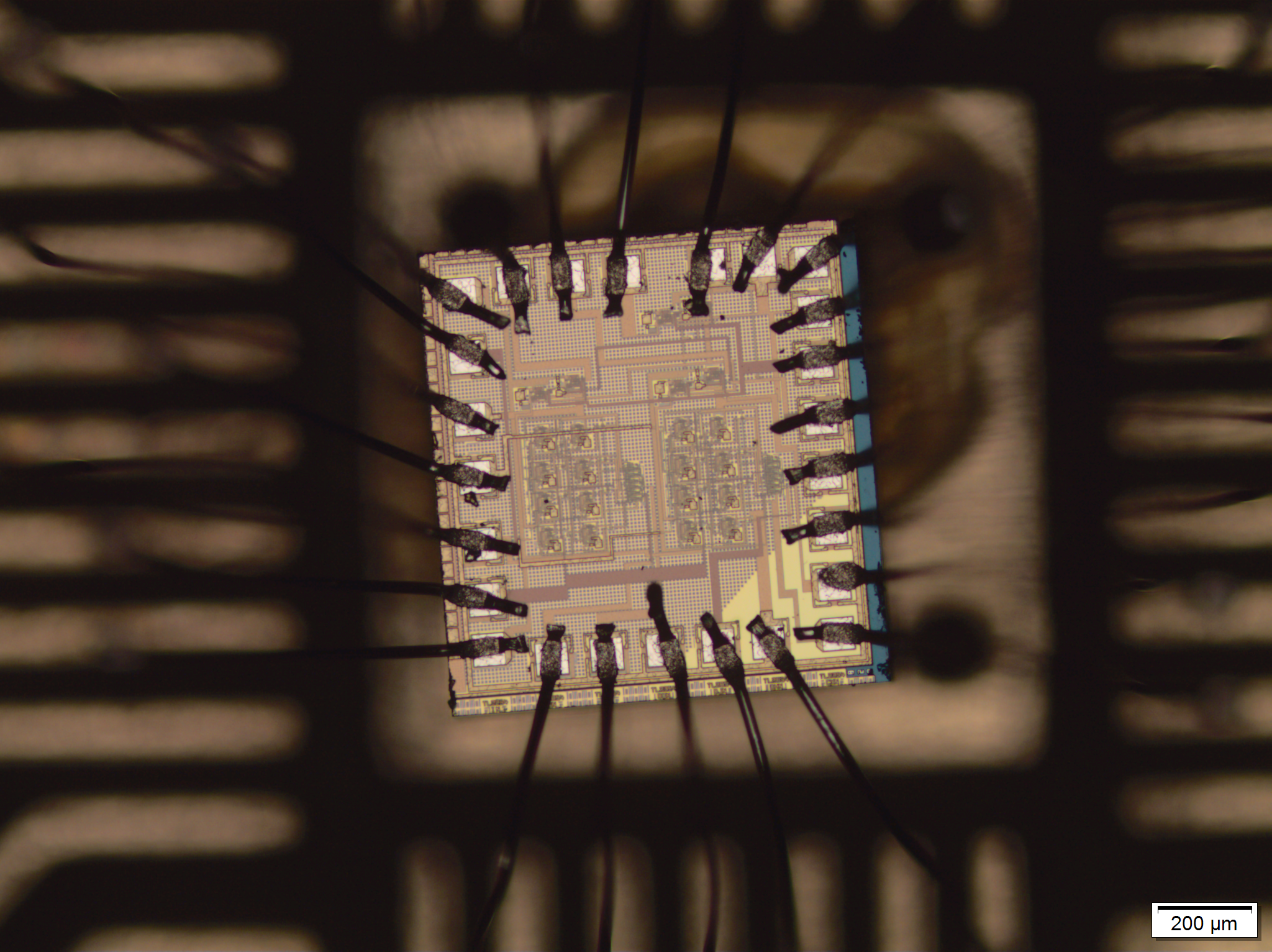
Our ferrodiode array under a microscope, wirebonded
-
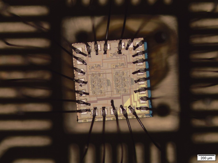
Our wirebonded chip under a microscope
-
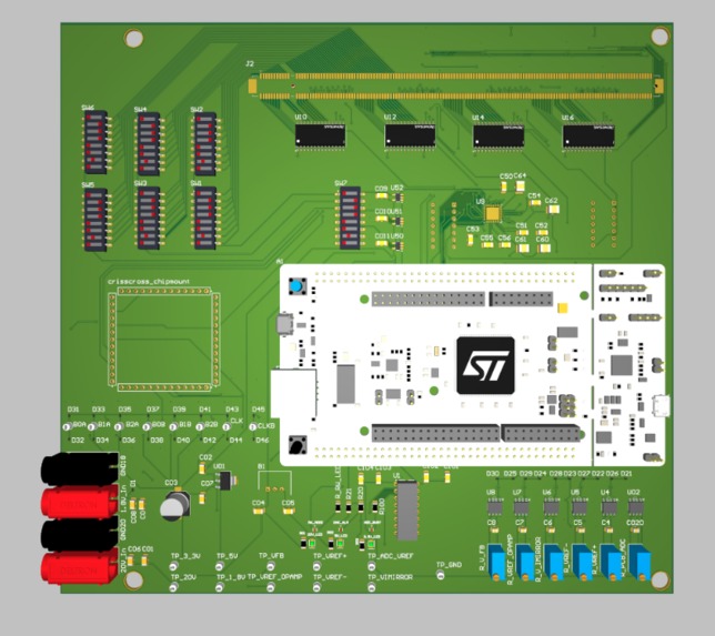
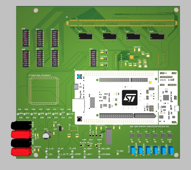
Our PCB
Inspiration
AI has an energy problem. Our AI energy footprint is the smallest it will ever be, and data centers already consume more energy than Canada, France, and Denmark do annually. We want to change the landscape of energy consumption by AI.
What it does
Matrix multiplication is the basis of AI computation, and consumes significant energy for training models. The time and power taken by these operations scale poorly with model size.
To solve this problem, we designed an end-to-end system to perform read and write functionality to/from the ferrodiode array, enabling less energy-intensive compute-in-memory matrix multiplication operations.
How we built it
Our system consists of an application-specific integrated circuit (chip) that performs current readout functionality, a PCB with an Arduino Giga R1 Wifi that allows us to interface our chip with the ferrodiode array, and firmware that controls the on-board pathways through the Arduino's MCU.
Challenges we ran into
The primary challenge we faced was interfacing with pico-level currents from the ferrodiode array and preserving signal integrity for downstream operations. Other logistical challenges included evolving chip area constraints on our circuit and PCB component selection for our boards.
Accomplishments that we're proud of
We successfully designed a chip in one month for fabrication. We achieved our desired objective of end-to-end system integration of the ferrodiode array, current readout chip, and the control PCB. We developed drivers of all on-board components and tested the functionality of our system individually and as a whole. Ultimately, we were able to read currents from the ferrodiode with an evaluation board which matched the expected behavior we sought out to demonstrate.
What we learned
Our major takeaway from this project is the importance of documentation to track key design reasoning and variables, thus creating a feedback loop that informs succeeding design decisions. Another important lesson for us is the creative problem-solving necessary to engage with novel technologies and highly sensitive devices.
What's next for CrissCross
Future iterations of the project will require continued experimentation with the chip in order to tune its functionality and observe desired behavior. A second iteration of the chip would include on-chip switches and muxes to reduce the data transfer rate between components on the PCB, thereby further reducing parasitics.


Log in or sign up for Devpost to join the conversation.