-
-
An introduction to Copper, a tool for PCB design analysis.
-
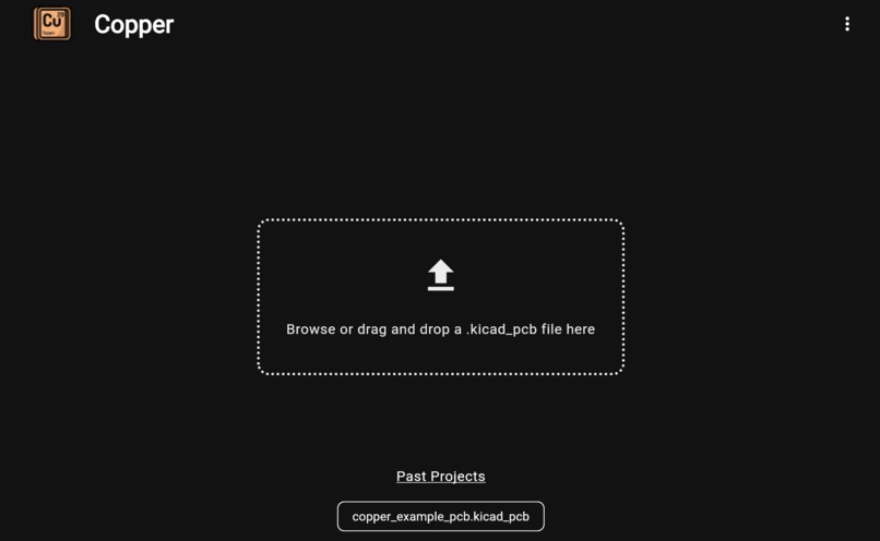
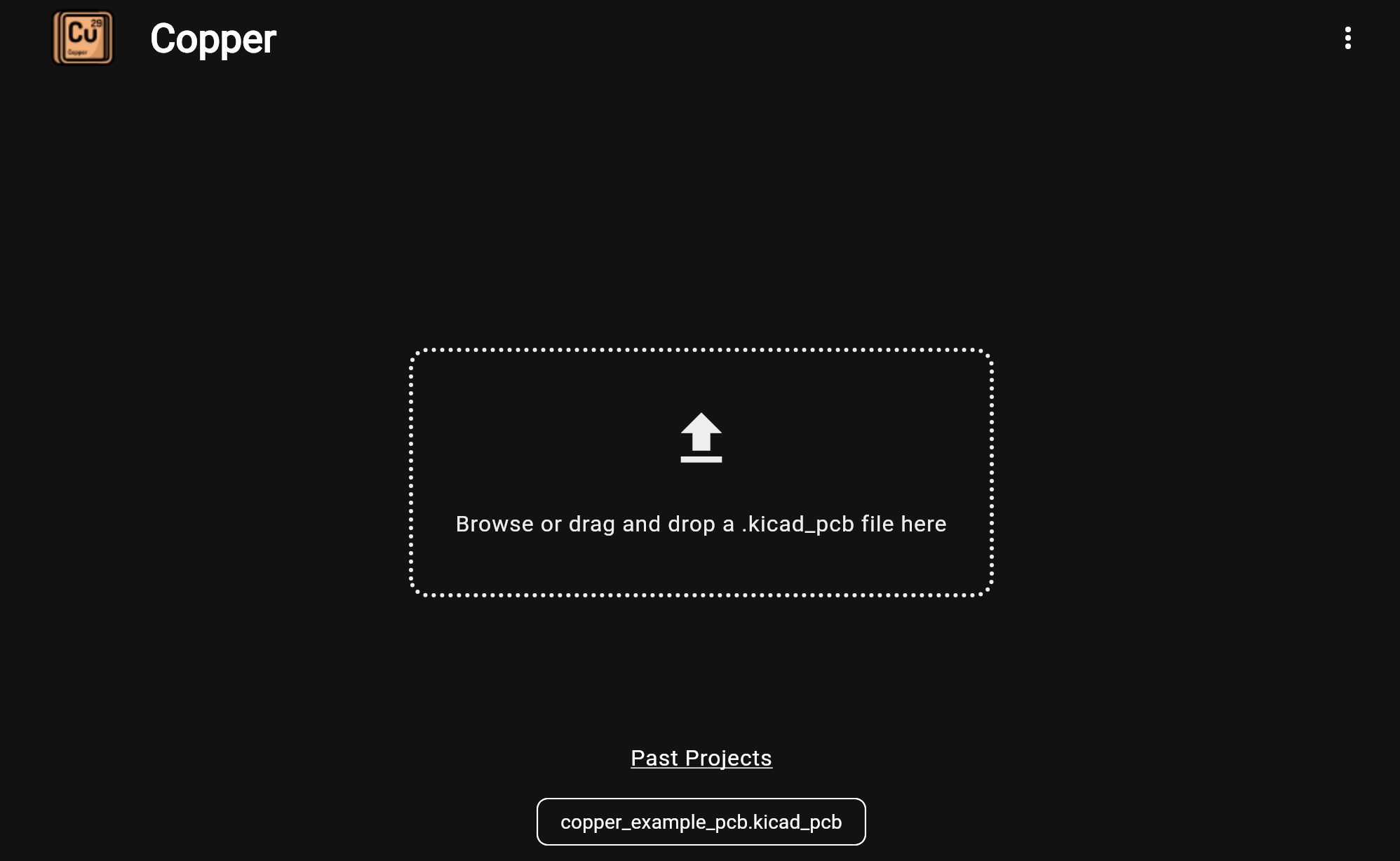
Start by uploading a PCB design.
-
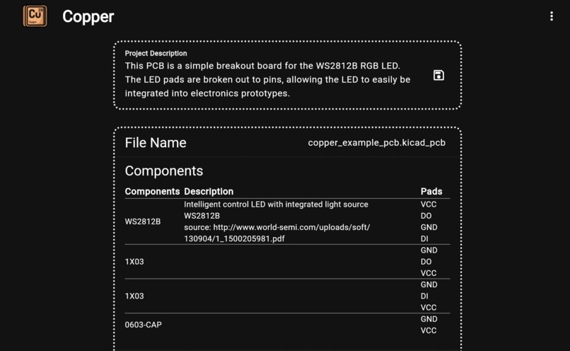
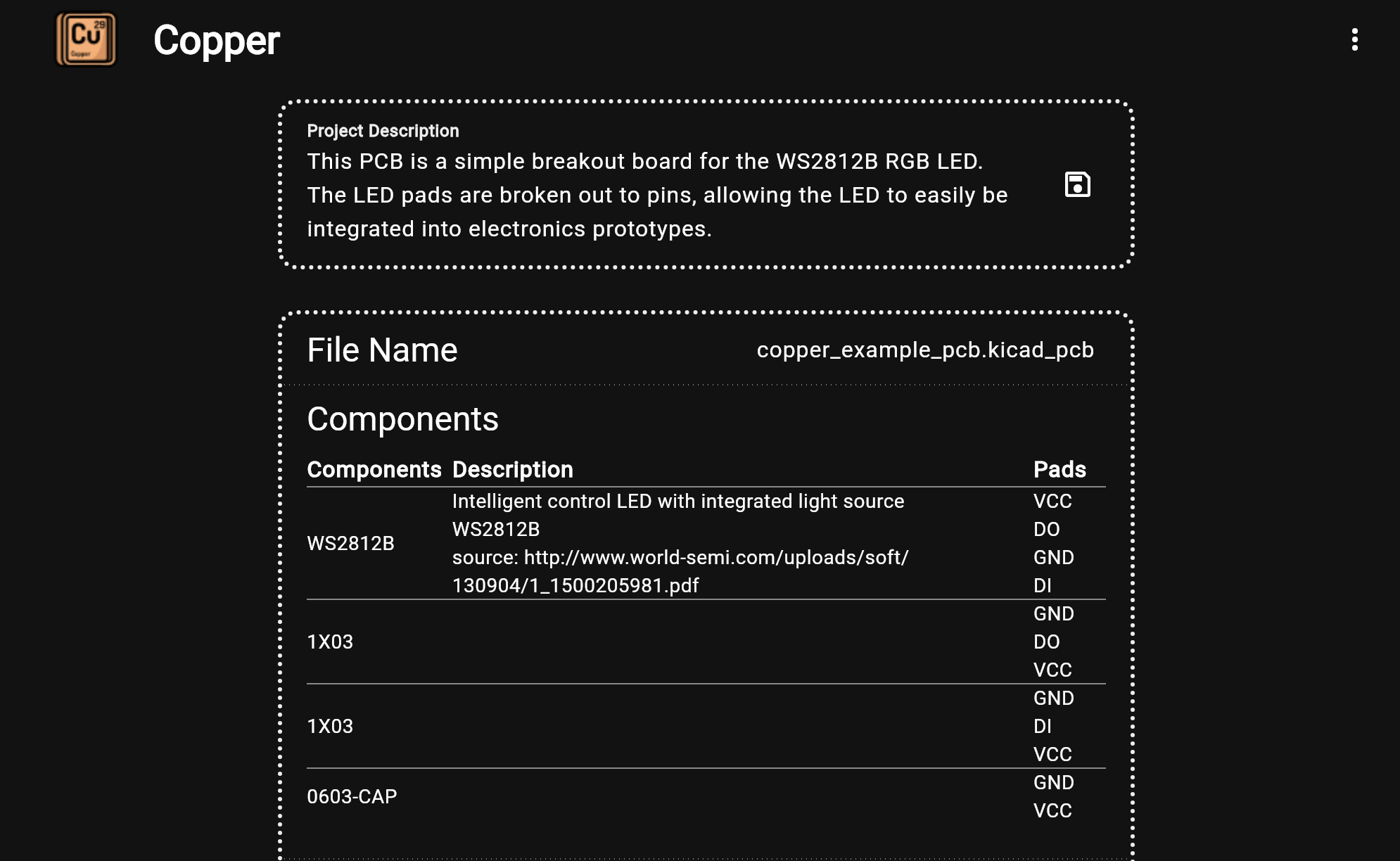
Get a snapshot of your design.
-
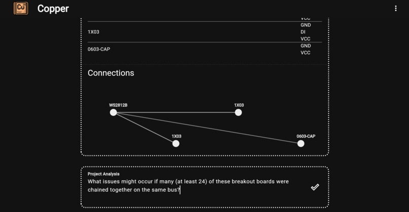
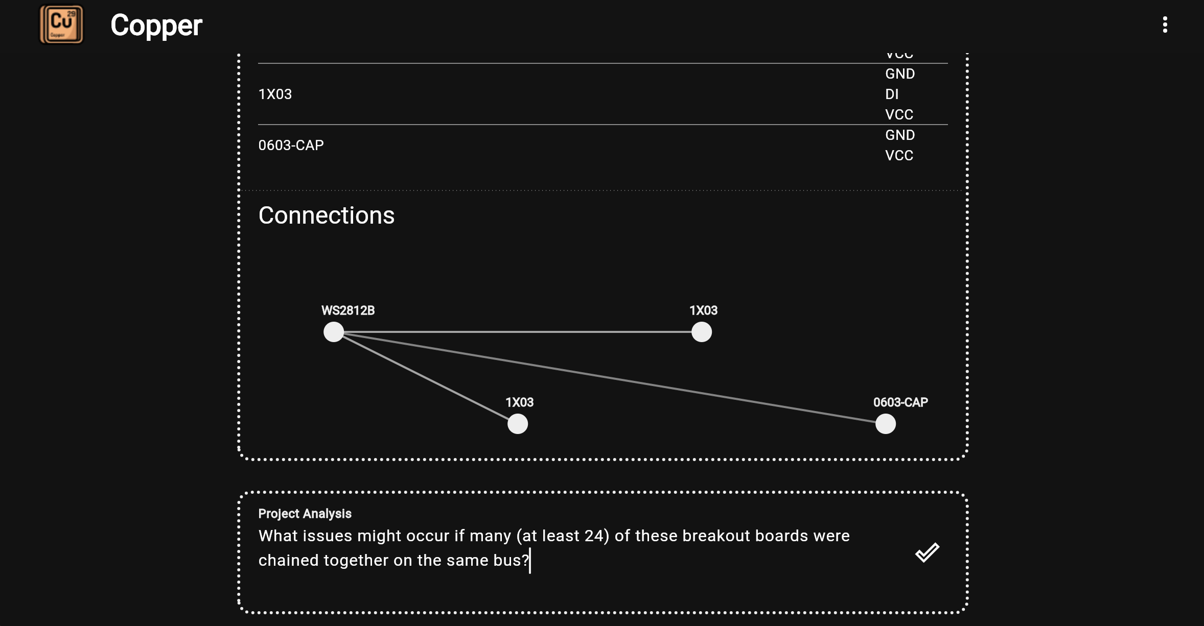
Ask prompts of the Copper system using natural lanauge.
-
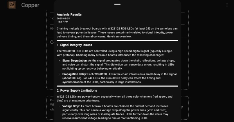
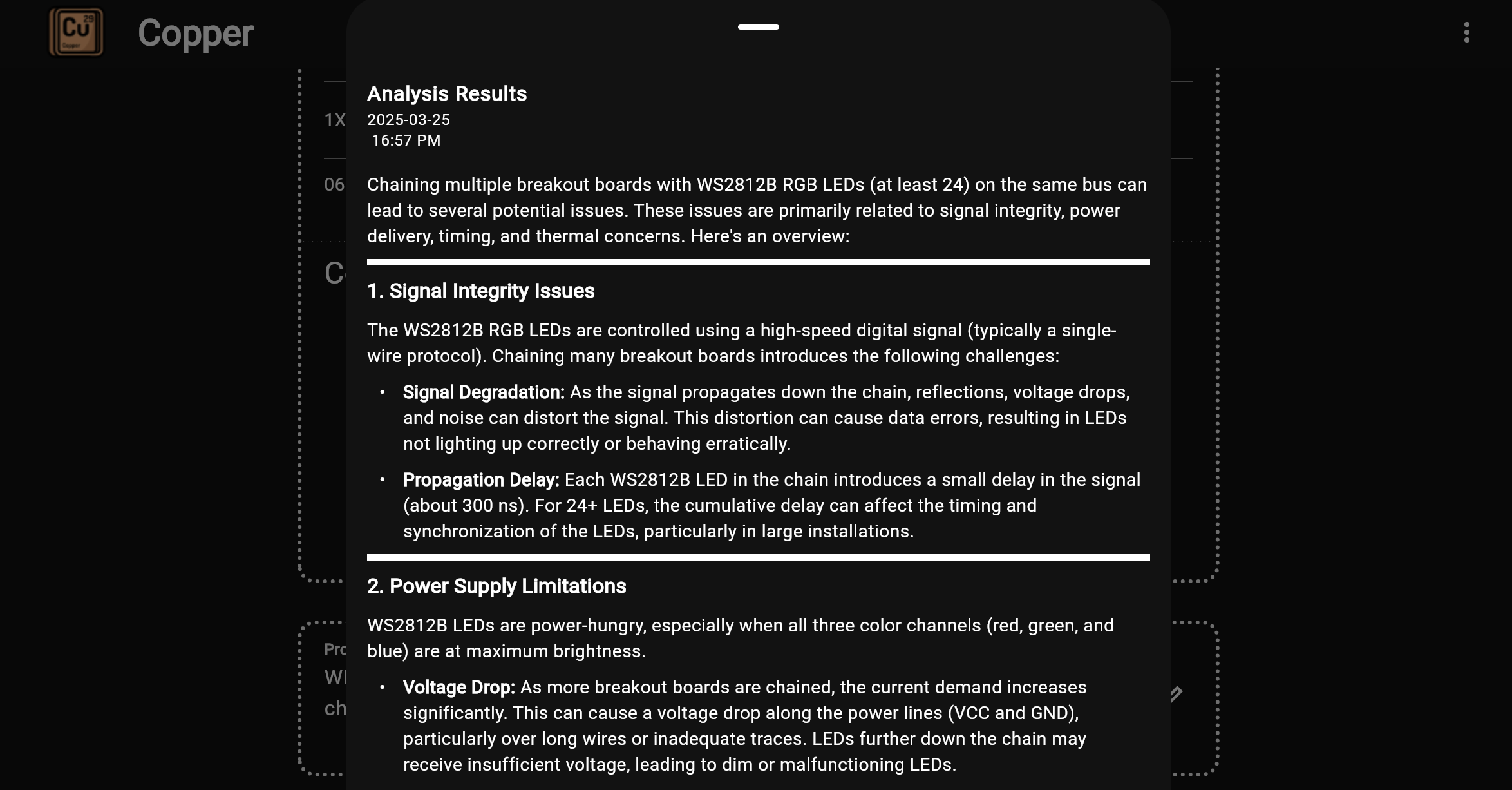
Receive analysis results to help you improve your PCB design.
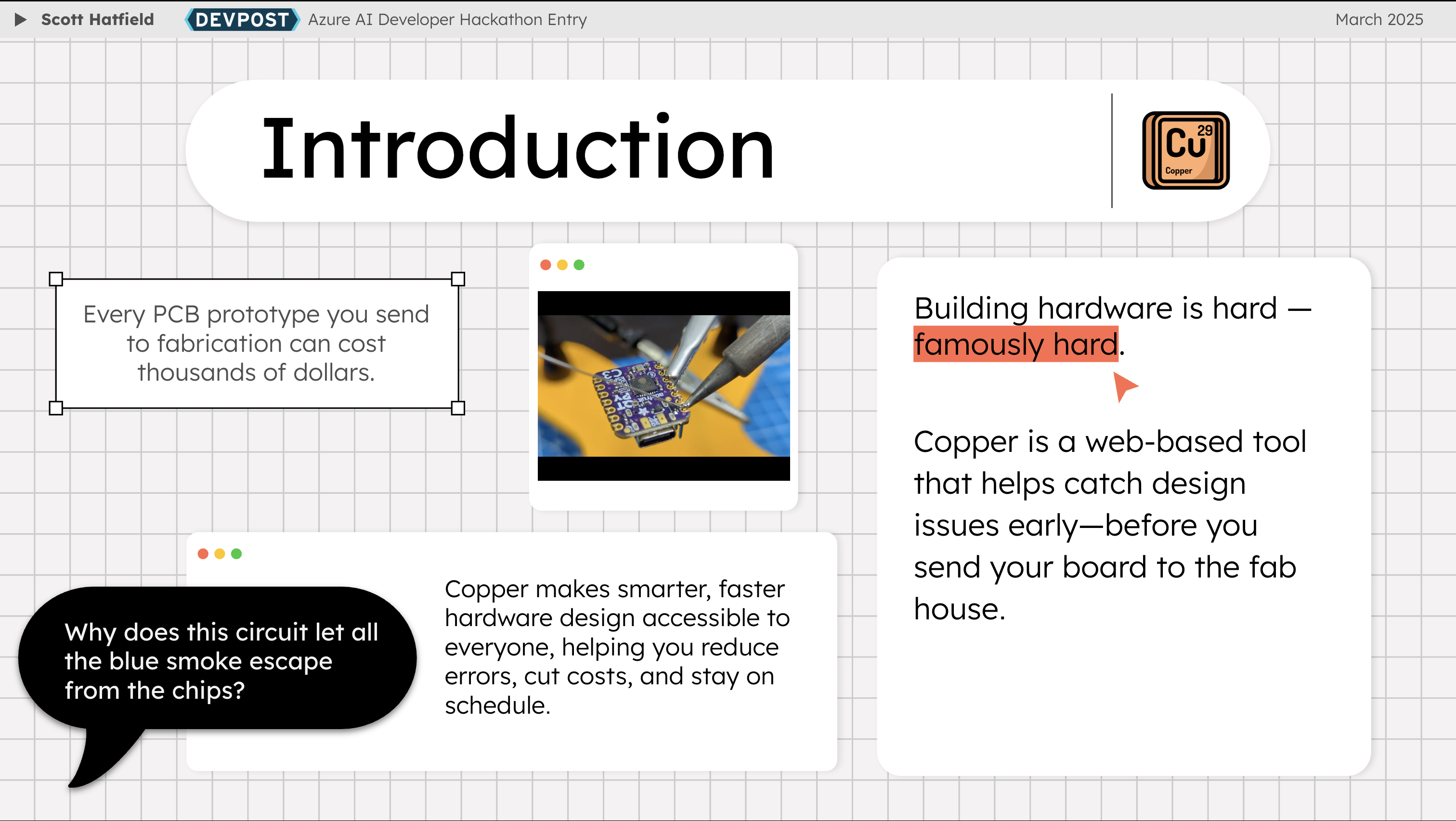
Inspiration: The Challenges of Building Hardware
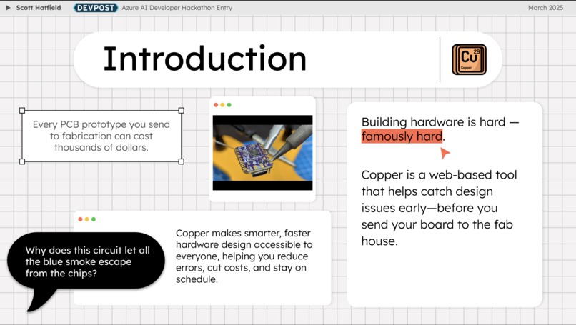
Building hardware is hard—famously, sometimes infamously, hard. Whether you’re in a startup garage or working in a massive enterprise, developing electronic products involves a long, expensive, and painstaking process. Unlike software, where fixes can be pushed in minutes, PCB (printed circuit board) development follows a much slower cycle. Designing a board, sending it for fabrication, waiting weeks for it to be manufactured and assembled, and only then testing it means that every mistake is costly—not just in dollars but in lost time.
Every prototype matters. A single design flaw can mean weeks of delay and thousands of dollars wasted. While working on electronics projects, I kept asking myself: Why isn’t there a better way to catch these issues before sending a board to manufacturing?
That question led to the development of Copper—a web-based tool that analyzes KiCad PCB designs using AI-powered insights, helping engineers catch and fix problems before committing to fabrication.
How Copper Was Built
To bring Copper to life, I leveraged Azure as the foundation of the infrastructure. Given the complexity of PCB analysis, cloud-based AI services were necessary to detect intricate design issues while maintaining a scalable backend for file parsing and reporting.
Tech Stack
- Flutter Web for a responsive and interactive frontend
- Azure AI Services for analyzing design rule violations, signal integrity risks, and manufacturability constraints
- Azure Functions to manage the backend processing of uploaded PCB files
- Azure Storage Containers for securely storing PCB design data and generated reports
The Workflow
- Uploading a Design – The user provides a
.kicad_pcbfile, which Copper parses to extract key design information. - Parsing the Design – The structured PCB data is parsed by the Copper app to produce an internal representation of the design data that allows for easier handling and manipulation within the app.
- Prompt Generation – The parsed PCB design data is used to create a prompt to be sent to an LLM in a natural language format that the LLM is better at processing. The PCB design data is combined with optional prompts by the user that allow for tailoring the analysis response to address specific areas or concerns within the design.
- AI-Powered Analysis – The structured PCB data is sent to Azure AI Services, where it undergoes analysis by the LLM system. Azure AI Services returns an analysis response in a structured data format.
- Generating a Report – A detailed report is compiled for display in the Copper app, highlighting design flaws and providing AI-generated recommendations for improvement.
- User Iteration – Engineers use Copper’s insights to refine their PCB before committing to manufacturing.
Challenges Faced
- Translating PCB Designs into an LLM-Understandable Format
One of the biggest challenges Copper had to overcome was how to present PCB design data in a way that a language model could process effectively. A previous experiment, documented in this Medium post, explored getting feedback on PCB designs by providing an LLM with screenshots of schematics or board layouts. This experiment was a failure because the LLM was not able to sufficiently understand the design from the images alone.
Copper solves this issue by extracting structured design data from .kicad_pcb files and converting it into a textual prompt that the LLM can interpret. Instead of struggling with pixel-based recognition, the AI is given a clear breakdown of circuit elements, netlists, and design constraints in a way that aligns with how it processes natural language. This transformation is key to making AI-powered PCB analysis feasible.
- Parsing KiCad PCB Data Efficiently
KiCad stores PCB designs in a structured, but complex, format. Extracting useful data—such as trace widths, netlists, and component placements—required building a robust parser that could process different versions of KiCad files accurately.
- Scaling AI-Powered Analysis
PCB designs vary wildly in size and complexity, from simple breakout boards to multilayer industrial designs. Running AI-powered rule checks at scale meant optimizing how data was fed into Azure AI Services while ensuring that processing times remained fast enough for an interactive user experience.
The Future of Copper
Copper is just the beginning of AI-powered PCB design analysis. The roadmap includes:
- Automated Fix Suggestions: Instead of just highlighting errors, Copper will suggest (and eventually apply) design fixes.
- Real-Time KiCad Plugin: A direct integration with KiCad for instant feedback while designing.
- Custom Rule Configuration: Allowing engineers to define their own DRC/ERC checks for tailored analysis.
- Support for Other EDA Tools: Currently, the Copper app only supports PCB designs created using KiCAD. In the future, the tool will be updated to support other PCB design file formats.
Conclusion
The process of building Copper reaffirmed an important reality: designing hardware is hard, but with the right tools, it can be easier. By integrating Azure AI Services, I have taken a step toward making PCB design smarter, reducing costly iterations, and empowering engineers to bring their hardware ideas to life faster than ever.


 Ho")


Log in or sign up for Devpost to join the conversation.