Inspiration
Hardware prototyping moves incredibly fast during hackathons, but the transition from a messy physical layout to a clean production schematic is a big challenge. After hand-wiring a dense multi-microphone array onto an STM32 development board, we realized how easy it is to lose track of connections amidst a sea of jumper cables. We wanted to build a tool that bridges the gap between physical prototyping and digital electronic design automation to allow hardware engineers to turn a simple smartphone photo of their assembly and/or .ioc file into a validated, production-ready PCB schematic instantly.
What it does
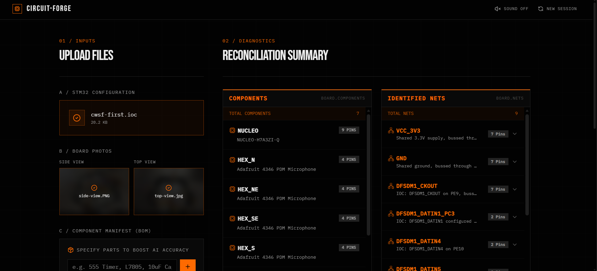
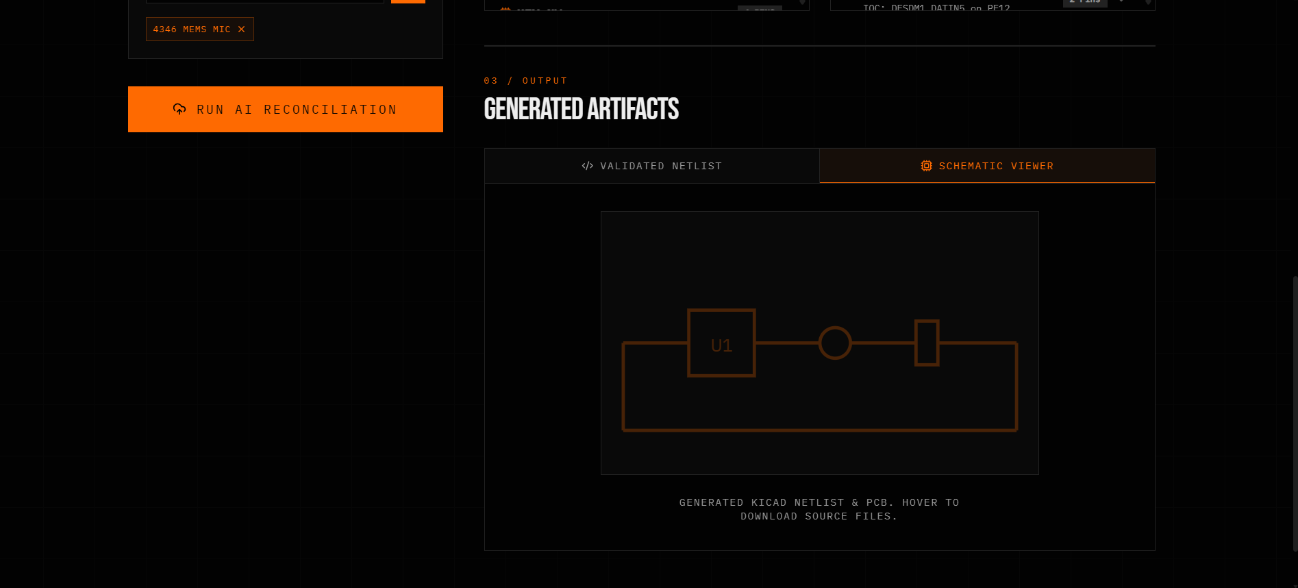
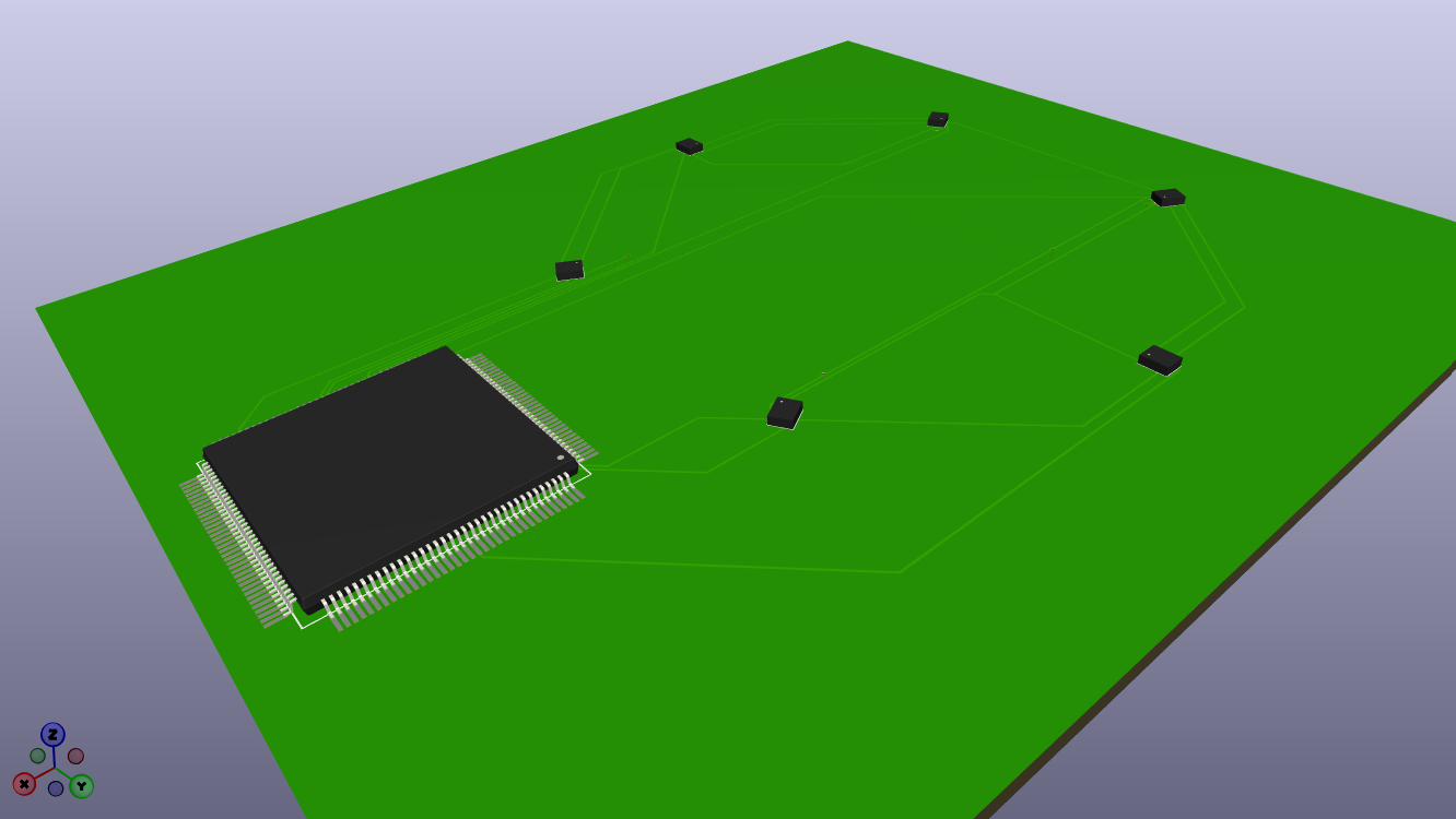
CircuitForge is an intelligent computer vision pipeline that analyzes photos of prototype hardware assemblies and automatically generates structured pin-level netlists and schematic files. By uploading images of a physical device alongside official pinout references, the platform actively maps out the system topology of the electrical networks. For example, we tracked a signal from the microphone breakout board, through a central custom power distribution perfboard and output a PCB board.
How we built it
We engineered CircuitForge using a modern, decoupled architecture split into an intelligent Python backend and a high-performance React frontend.
- Backend (Python, FastAPI): The application is powered by a FastAPI REST server. When a user uploads a hardware photo or an STM32 CubeMX .ioc file, the image is processed using Pillow and sent to the Google Gemini API (gemini-2.5-flash and gemini-3.5-flash). The LLM performs computer vision analysis to execute multi-modal inference, parsing the STM32 pin configurations, identifying components, and mapping the physical wire connections.
- EDA Generation: The backend synthesizes the output of the vision pipeline and .ioc data into a unified netlist. Using the pure Python standard library (math, pathlib, json), we programmatically generate native KiCad .net files for schematic import, alongside fully structured KiCad .kicad_pcb layout files. These files contain precise definitions for component footprints, pads, and courtyard layers, with placement inference enhanced by the Gemini API. We also integrated a DigiKey API client layer to enrich the generated BOM with component metadata.
- Frontend (React, Vite.js, TypeScript): We built a highly responsive, minimalist dashboard optimized for engineering workflows. File uploads are handled smoothly via react-dropzone. The user interface leverages Tailwind CSS v4 for clean, modern styling, combined with a sophisticated animation stack featuring Framer Motion, GSAP, and Lenis smooth scrolling to deliver fluid visual feedback during intensive compilation and rendering steps.
Challenges we ran into
- One of the most complex hurdles was resolving multi-modal data synchronization. Reconciling high-level visual data from a smartphone camera with the strict, deterministic plaintext format of an STM32 .ioc initialization file proved incredibly challenging.
- Another challenge was when we discovered that relying on a single camera angle was highly unreliable for computer vision processing. Capturing the assembly from just one perspective led to massive wire occlusion issues, where overlapping jumper cables completely blocked the Gemini API from seeing underlying connections and pin labels. To solve this, we pivoted to a multi-angle approach, requiring both a top-down structural shot and a side-angle perspective. Fusing these two distinct visual viewpoints with the text-based .ioc pin configuration data forced us to build a far more sophisticated spatial reconciliation pipeline, ensuring the LLM could accurately trace a wire from its source to its destination without getting tripped up by perspective distortion.
Accomplishments that we're proud of
We are incredibly proud of building a compiler that successfully outputs syntactically valid, production-ready KiCad hardware files from unstructured visual inputs. Successfully mapping an arbitrary physical wiring setup all the way to structured .net and .kicad_pcb files felt like magic. What made it even more rewarding was successfully rendering this complex architectural data within our web interface, allowing users to inspect their generated boards seamlessly in both 2D layouts and fully interactive 3D space.
What we learned
This project gave us deep insight into the practical application of multi-modal generative AI within hardware engineering. We learned how to structure robust prompts to extract precise, deterministic spatial and electrical connection data from visual assets. We also gained a comprehensive understanding of the internal structure of electronic design automation (EDA) files, recognizing that hardware layouts can be treated as abstract data graphs that are open to algorithmic optimization.
What's next for Circuit Sync
While the Gemini API provided an incredible foundation for multi-modal prototyping, the next step is to transition to dedicated, edge-optimized computer vision models to achieve the millimeter-level precision required for complex engineering tasks. We plan to build a custom visual pipeline specifically trained on electronic component packages and wire tracing. This will allow us to scale up to massive, multi-layer hardware assemblies, refining our multi-angle photography framework to definitively eliminate wire occlusion and automatically map stacked breakout boards. Ultimately, we envision CircuitForge evolving into a robust, real-time bridge from a physical workbench to an automated manufacturing line.
Built With
- digikey
- fastapi
- gemini-vision-api
- python
- react
- tailwind
- typescript
- uvicorn
- vitejs


Log in or sign up for Devpost to join the conversation.