-

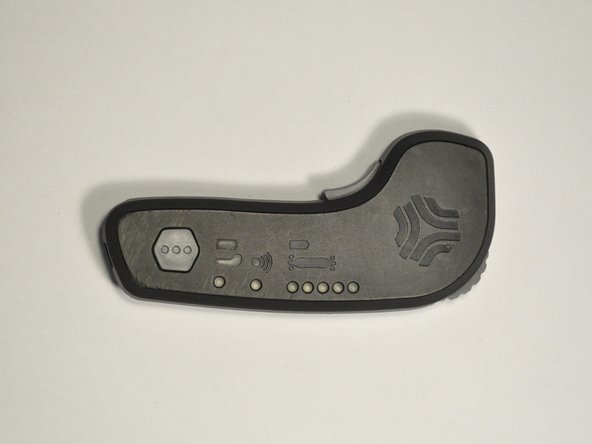
Original Boosted Boards remote
-

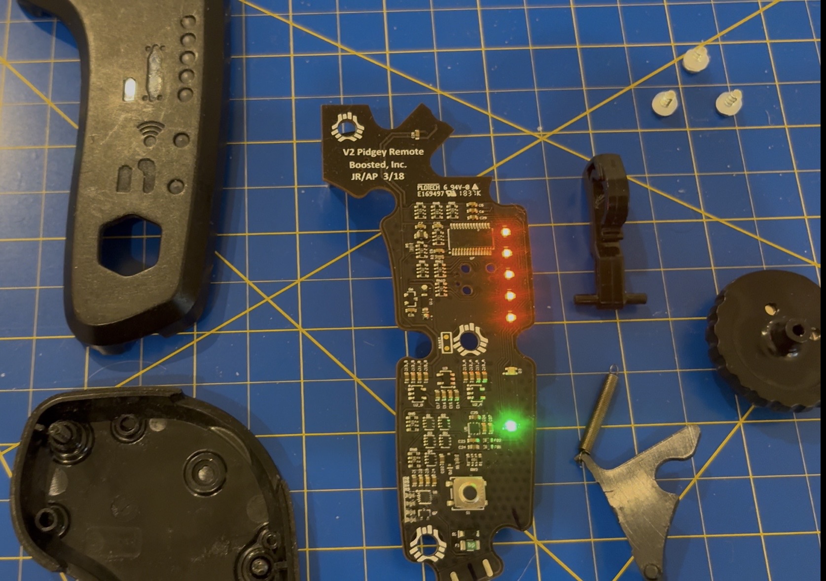
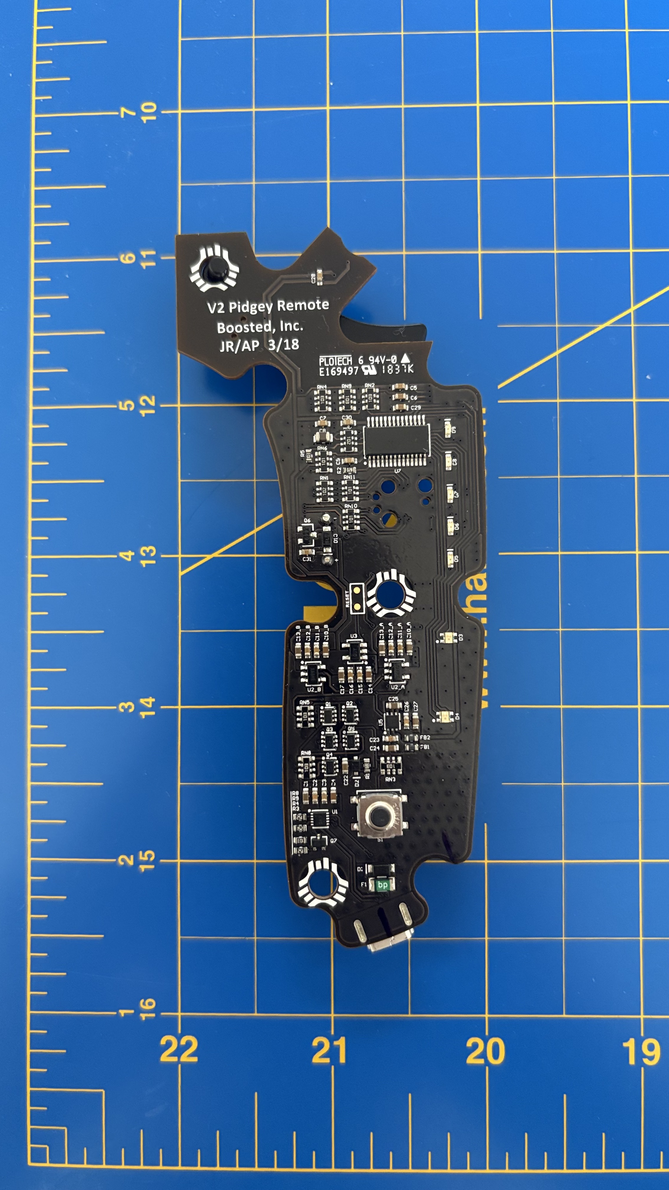
Original remote teardown
-
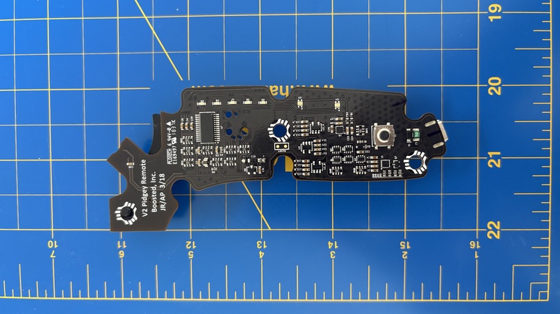
Original remote PCB
-
-

Redesigned electrical schematic
-
-
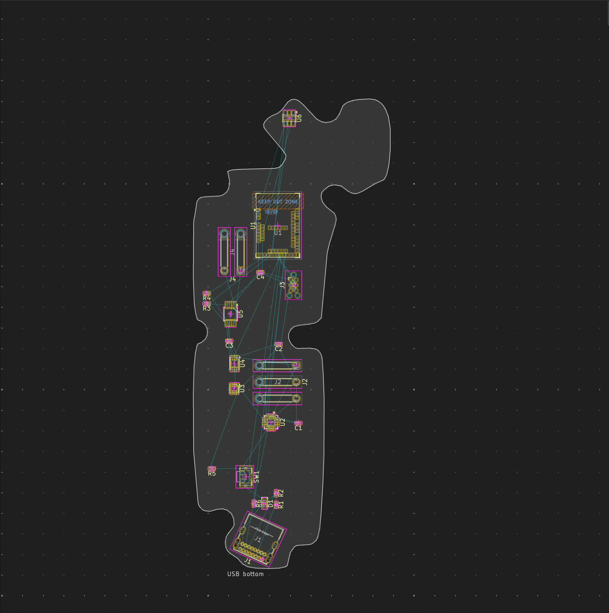
Layout
-
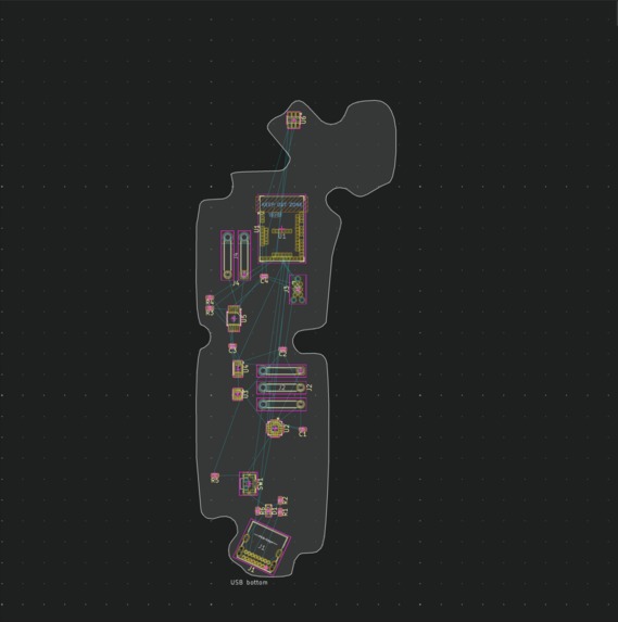
Ratsnest
-
 GIF
GIF
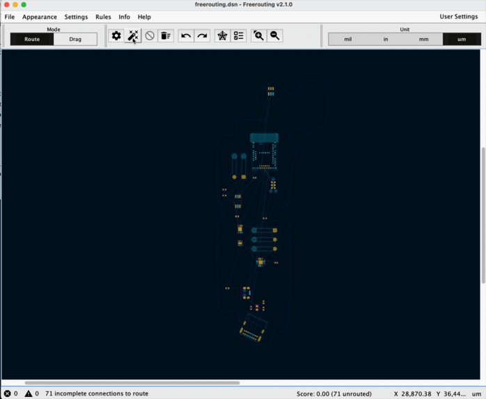
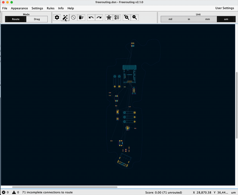
Routing with the Freerouting KiCAD plugin
-
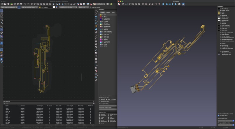
Front copper
-
Back copper
-
Fully layers
-
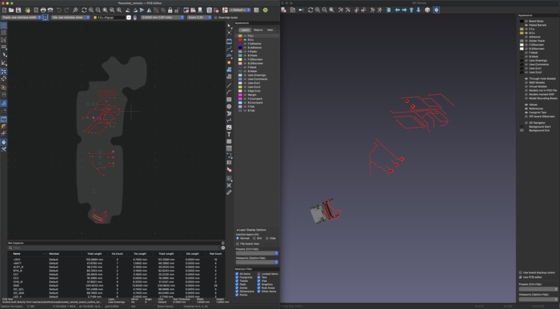
Design rule checker green
-
-

Fabrication
-
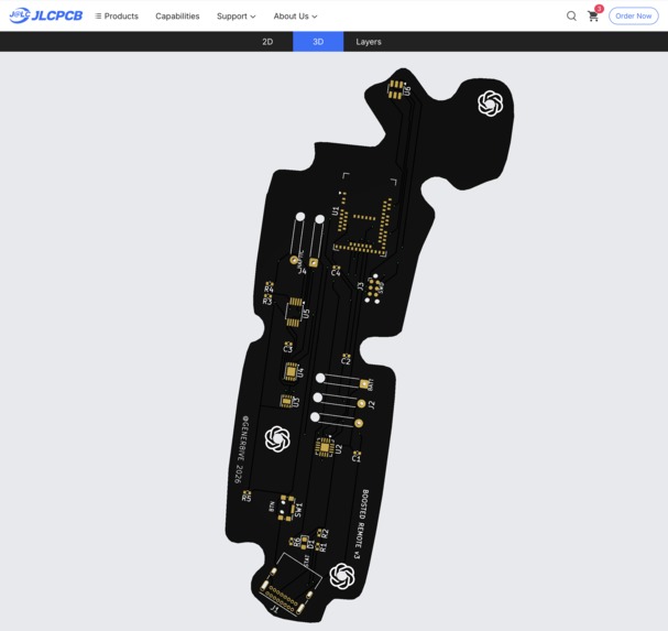
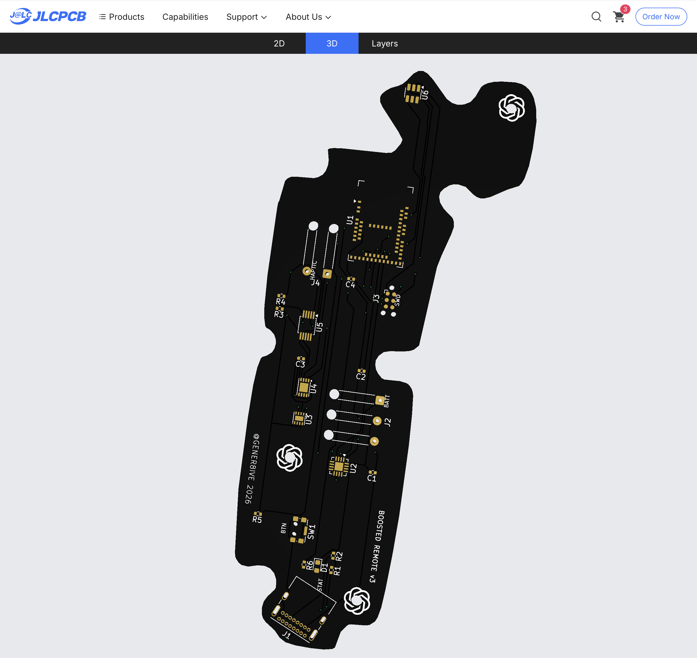
JLCPCB Render 1
-
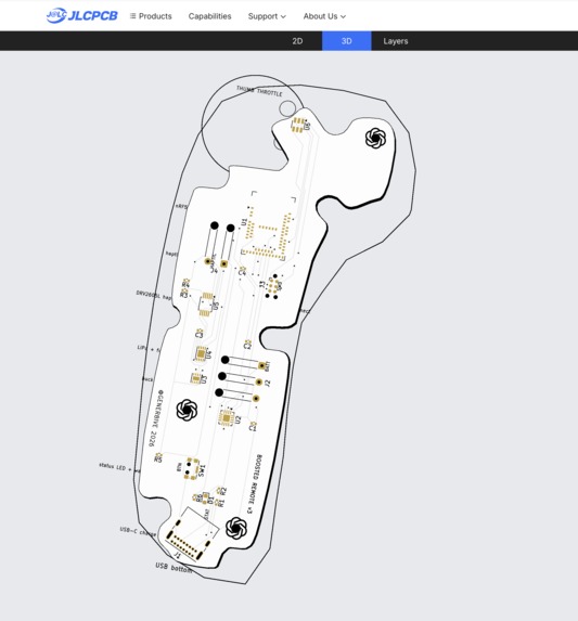
JLCPCB Render 2
-

Prompt snippet #1
-

Prompt snippet #2
-
Prompt snippet #3
-
Prompt snippet #4
As a hardware hobbyist who's tinkered with Arduino and Raspberry Pi for years, I generally assumed that custom PCB design was out of reach due to the electrical engineering and CAD expertise required.
Then one day a few weeks ago, two things dawned on me:
- Frontier coding models like Codex & Claude have likely read every electrical engineering textbook and open source electronics repo in the world. At least enough to have learned the principles of electrical engineering to a high level of competency.
- Behind every button inside a CAD program's UI is a function. If the software has a good scripting interface like a CLI or Python interpreter, Codex should be able to write code to call that function and interact with it in a loop.
I figured:
"What if we gave Codex the tools an electrical engineer or PCB designer actually uses?"
Google, KiCAD, and some kind of a debugger seemed like a good place to start.
In this write-up, I'll show how that intuition proved to be unreasonably effective. The focus is the Boosted Boards remote, but the concepts of how to use coding agents for electrical (and mechanical) design should be generally applicable.
TLDR: with the right set of CAD tools and a scripting interface (CLI/Python Interpreter, etc.), a frontier coding agent like Codex/GPT-5.4 or Claude Code/Opus 4.6 can can accelerate the design a printed circuit board (PCB) including parts selection, schematics, electrical and design rule checking, layout, and routing. While this approach likely won't work for more complex board designs at the moment, the direction appears to be clear - agents can (co)-design some boards.
Agentic Electric Design
Step 1: Braindump
As with any design project, it starts with an idea. Not too big, not too small. "Rebuild the Boosted Board electric skateboard"? Too big. "Design a simple circuit to learn 'the basics'?" Too small. "Reverse engineer the v2 Boosted Boards electric skateboard remote." Just right.
I'm a big fan of the idea dump at the start of a project with agents. Once you have an idea of what you want to build, start dumping ideas and images into a workspace that you can share with the agent as starting context.
Step 2: Structured Design Spec
Work with the agent to create a structured design spec for the braindump from Step 1. Written in JSON, the file is used by a Python generator script to create the *.kicad_sch and *.kicad_pcb files in KiCAD according to the design specification.
{
"project_name": "boosted_remote",
...
"electrical": {
"battery": "1S LiPo 400-600mAh",
"mcu": "ESP32-C3-WROOM-02",
"charger": "MCP73831-2-OT",
"regulator": "TLV75533PDBV",
"hall_sensor": "DRV5055A3xDBZxQ1",
"charge_current_ma": 212,
"programming_header": "UART_1x06_1.27mm"
},

"pinout": {
"hall_adc": "IO4",
"deadman_switch": "IO5",
"power_button": "IO6",
"buzzer_drive": "IO7",
"status_green": "IO8",
"status_blue": "IO9",
"led_bar_1": "IO10",
"led_bar_2": "IO18",
"led_bar_3": "IO19",
"led_bar_4": "IO3",
"led_bar_5": "IO2",

"battery_sense": "IO1",
"boot": "IO0",
"uart_rx": "IO20/RXD",
"uart_tx": "IO21/TXD"
}

}
Step 3: Mockups
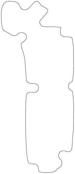
Generate visual mock-ups, sketches, drawings, etc. of the proposed design to get a rough visual idea of what you and your agent are trying to build.
Even though though I tried to separate the mechanical work from the electrical, having an outline of the remote's outer shell was a helpful reference.


Step 4: Plan
With the mock-ups and structured design spec, ask Codex to write a plan to use the KiCad CLI to iteratively design & test the proposed PCB.
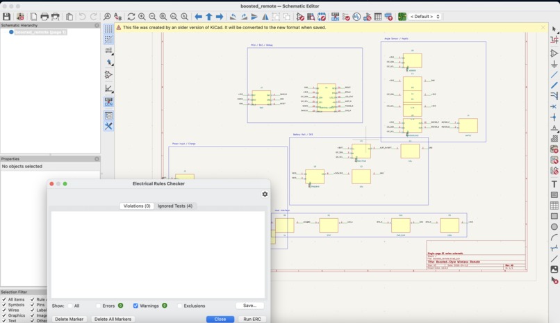
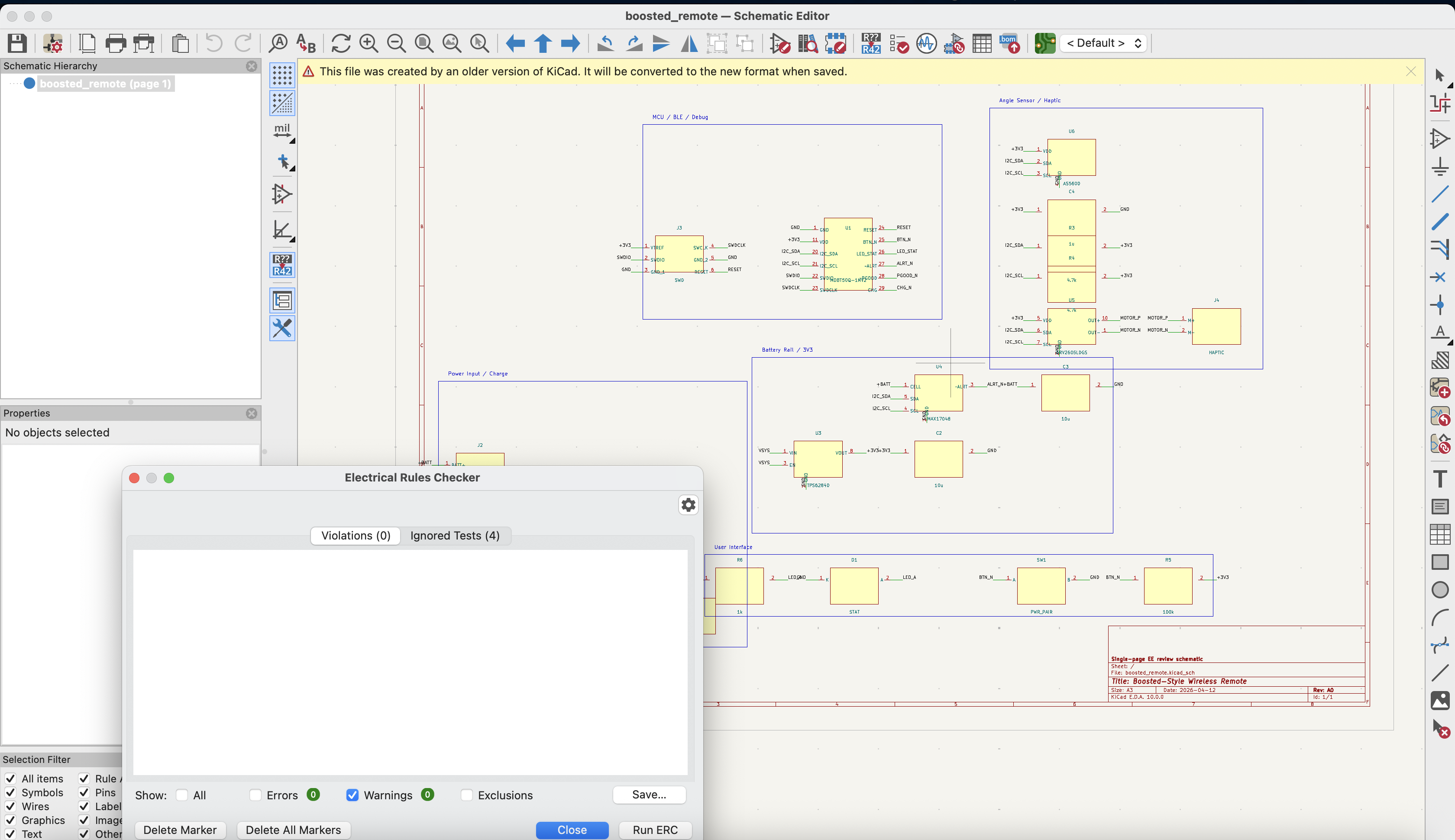
Step 5: Schematics
From the plan, create the electrical schematic. Get Codex to run the electrical rule checker (ERC) and iteratively fix violations before moving on to layout, placement, and routing.
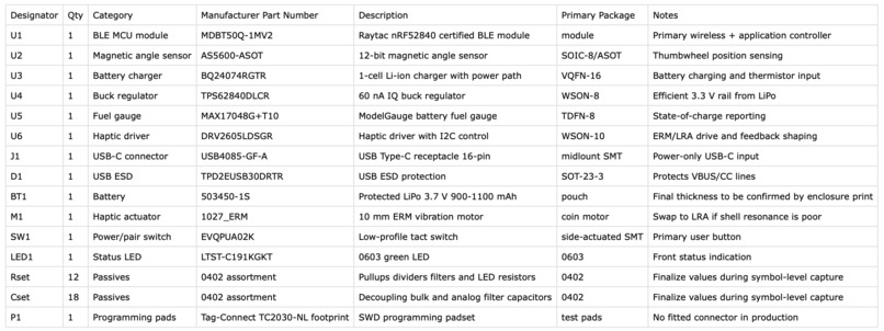
Step 6: Bill of Materials
From the schematic, craft the BOM.

Step 7: Layout
From the BOM, mockups, schematic, and structured design spec, lay out the electrical components at the zone and layer level within the constraints of the mechanical envelope/enclosure.
Step 8: Routing
With the board laid out, it's time to start routing.
I used the Freerouting KiCad plugin to auto-route the board, but ran into a bunch of problems I had to find ways around.
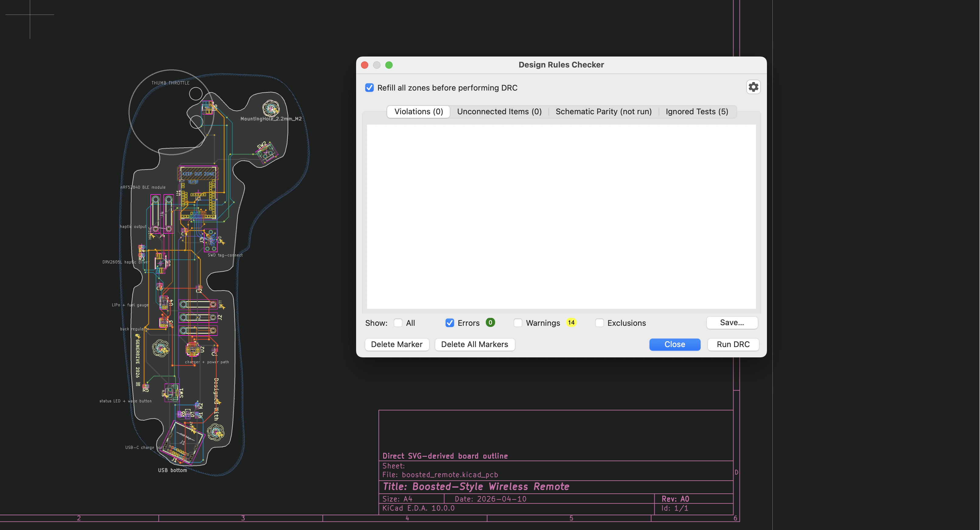
Similar to the electrical rule checker loop for our schematic, I ran the design rule checker (DRC) in a loop to iteratively flag and fix design rule violations. I instructed Codex to repeat the loop until there were zero errors or it hits a wall and needs me to manually route or place components. (Screenshot below is of me pointing & clicking inside the Freerouting UI, but Codex can run this in a terminal inside its agent loop then inspect and iterate on its errors).
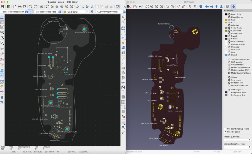
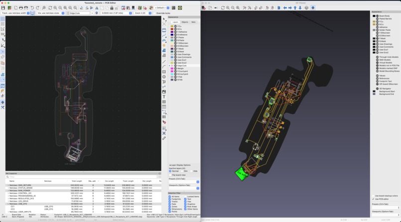
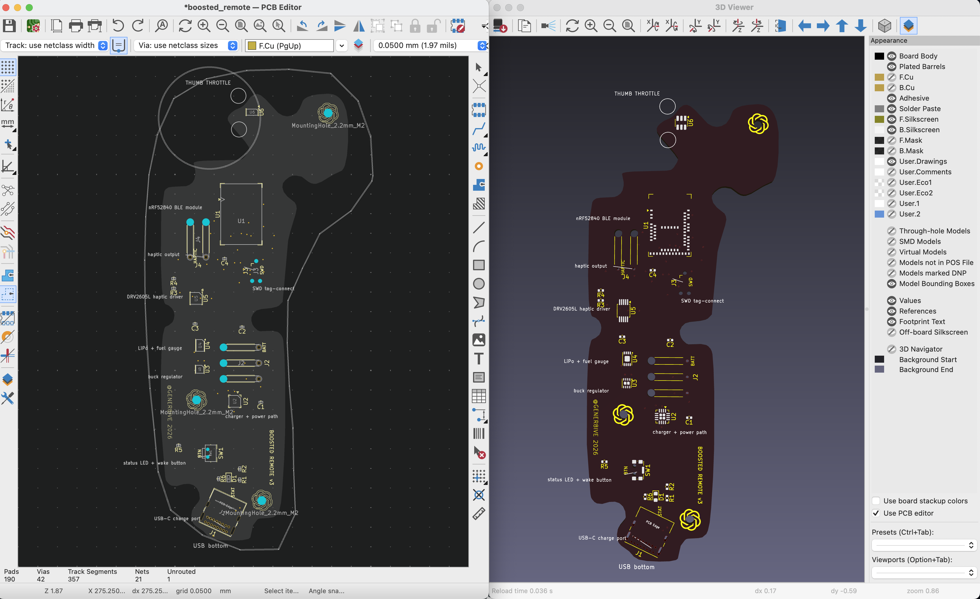
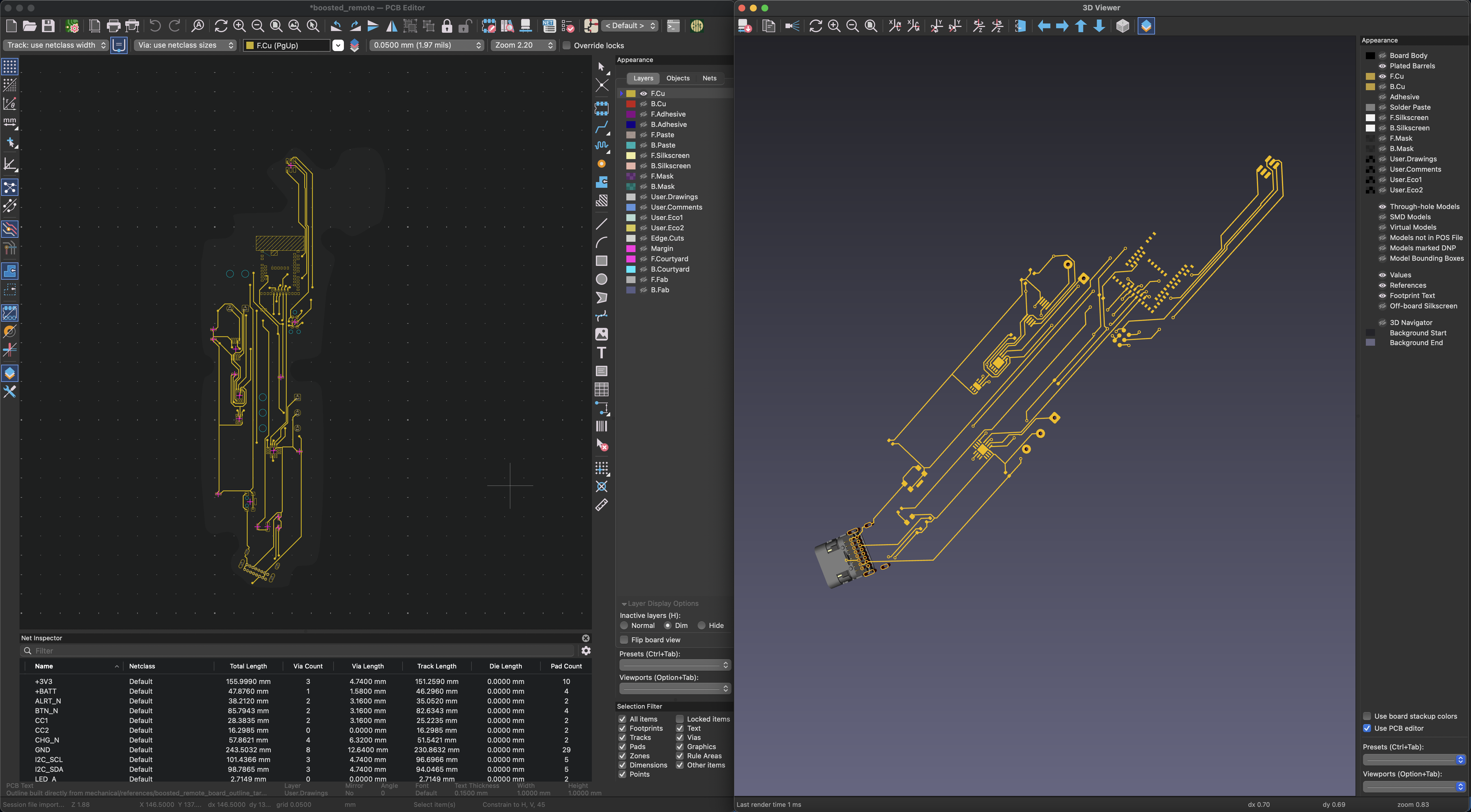
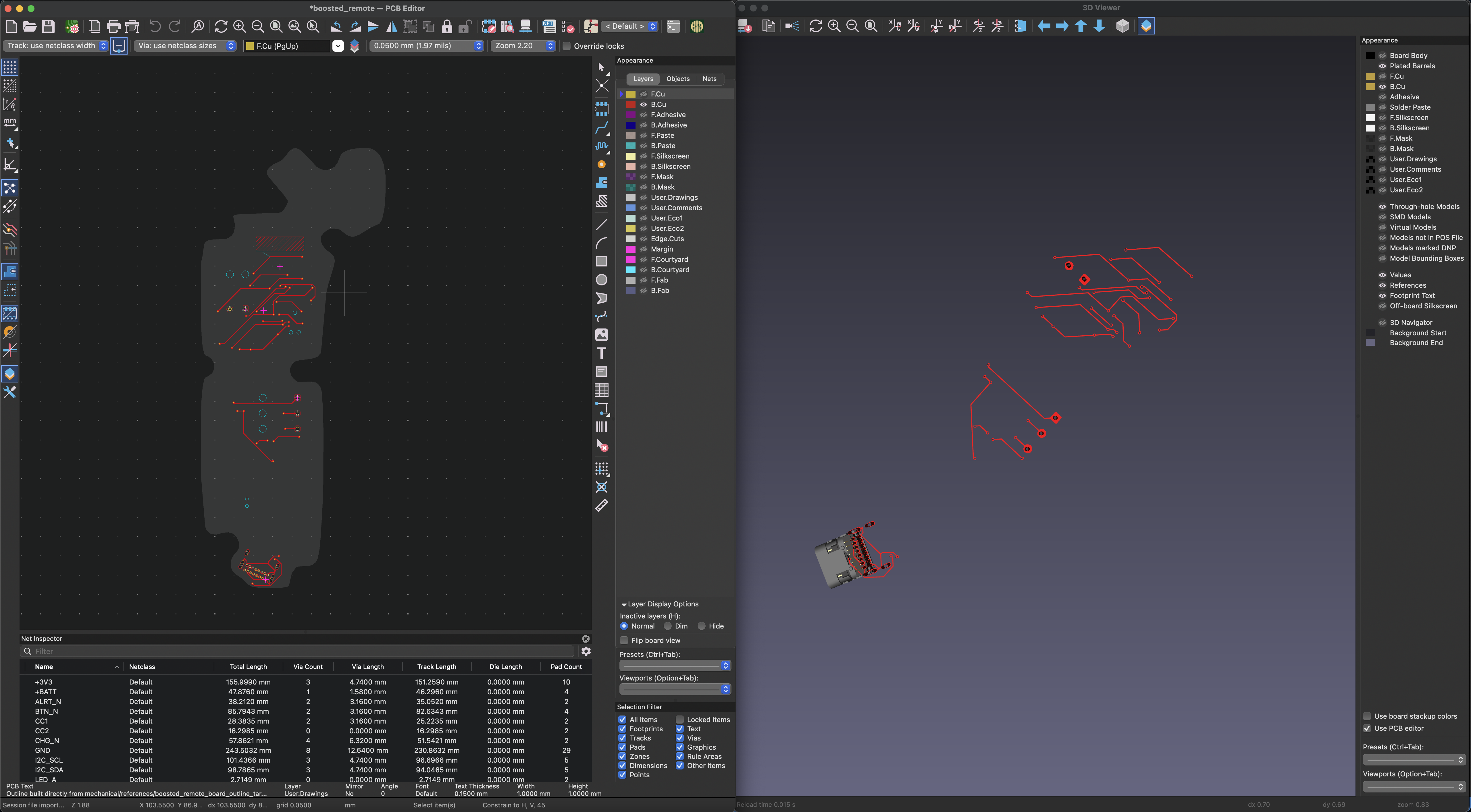
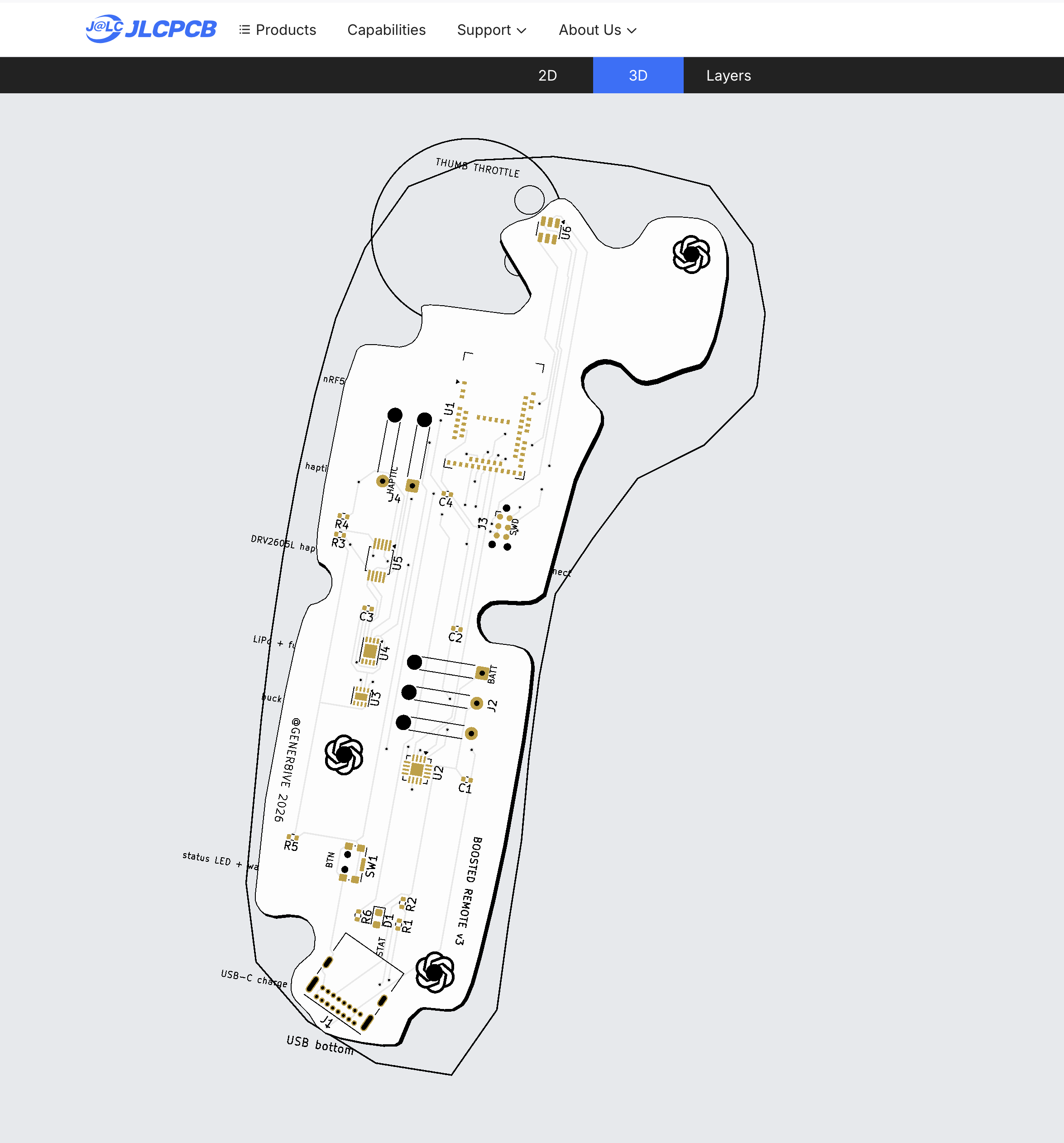
Copper Layers
Even if routing completed successfully with 0 errors, it's still wise to inspect the board using KiCAD's visual inspection tools. KiCAD's PCB Editor and 3D Viewer are super helpful in visualizing the board many layers - front/back copper, footprints, silkscreens, courtyards, edges, solder masks, and many other. What on the surface is super complex, can be filtered, and edited to focus-in on the circuit
Fully Layered Board
By categorizing the different components and traces into 'netclasses' I was able to make the circuit's form and function much more apparent. Colour-coded netclasses in particular were a useful trick for quickly seeing what components were connected (or not).

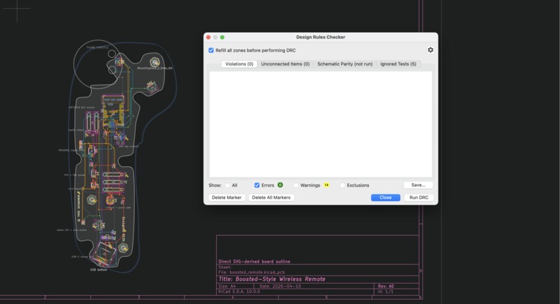
Design Rule Checker (DRC) After routing, run DRC and iterate (with the agent & manually) to resolve errors. I found this process to be very similar to running a type checker or linter in a software project. The visual cues (yellow & red arrows) help to navigate and identify what needs to be fixed (although, the agent just uses coordinates).
Step 9: Export & Upload
In order to print the board, the fabricator (fab) needs what are known as Gerber files - basically a zip folder with each of the layers exported from KiCAD or whatever EDA tool you're using.
JLCPCB's Board Uploader
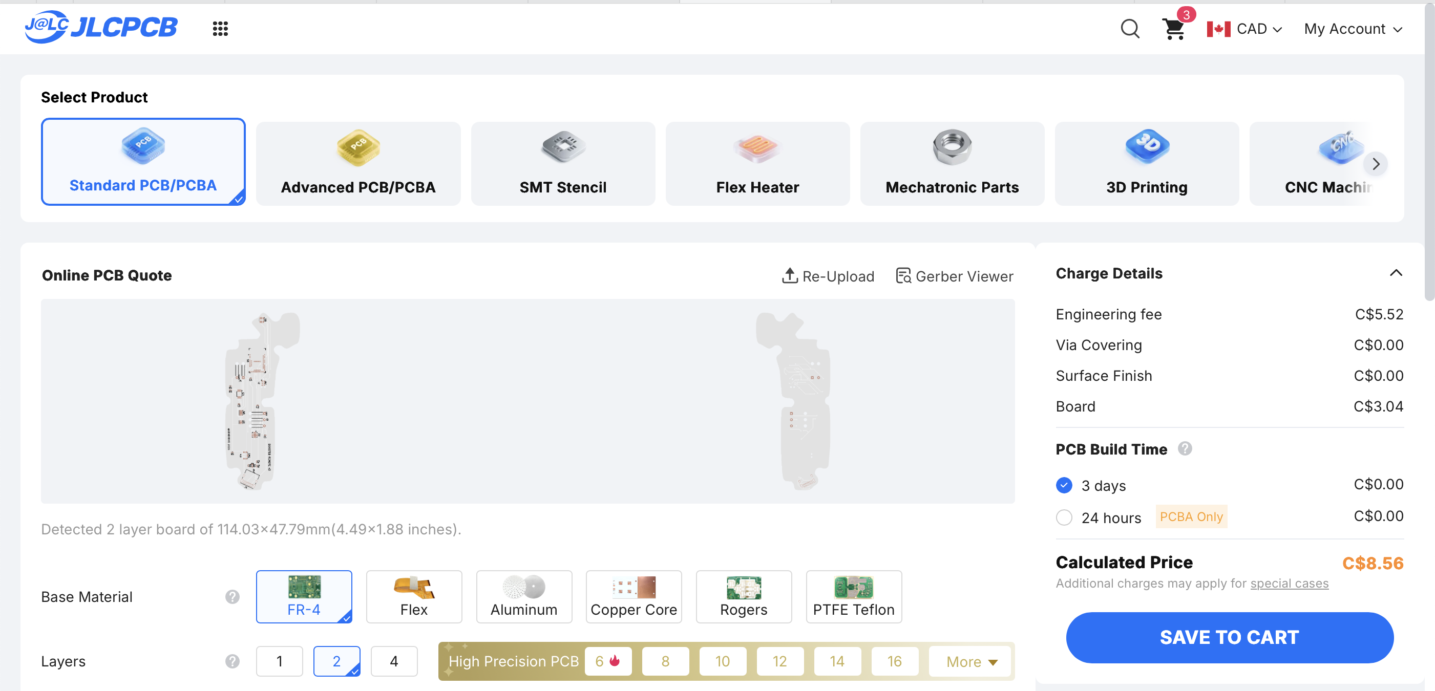
JLCPCB's Gerber Viewer
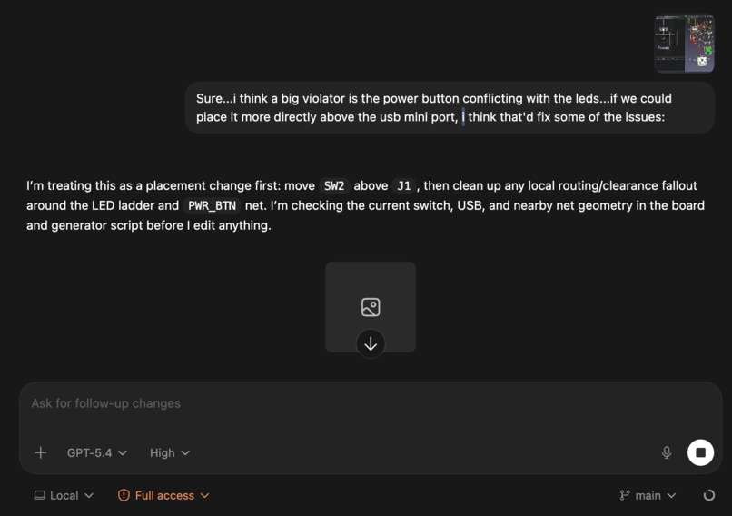
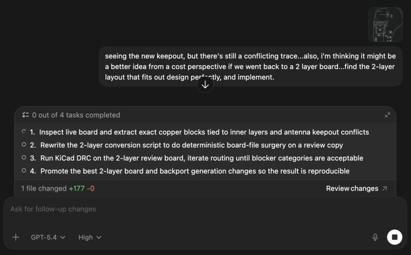
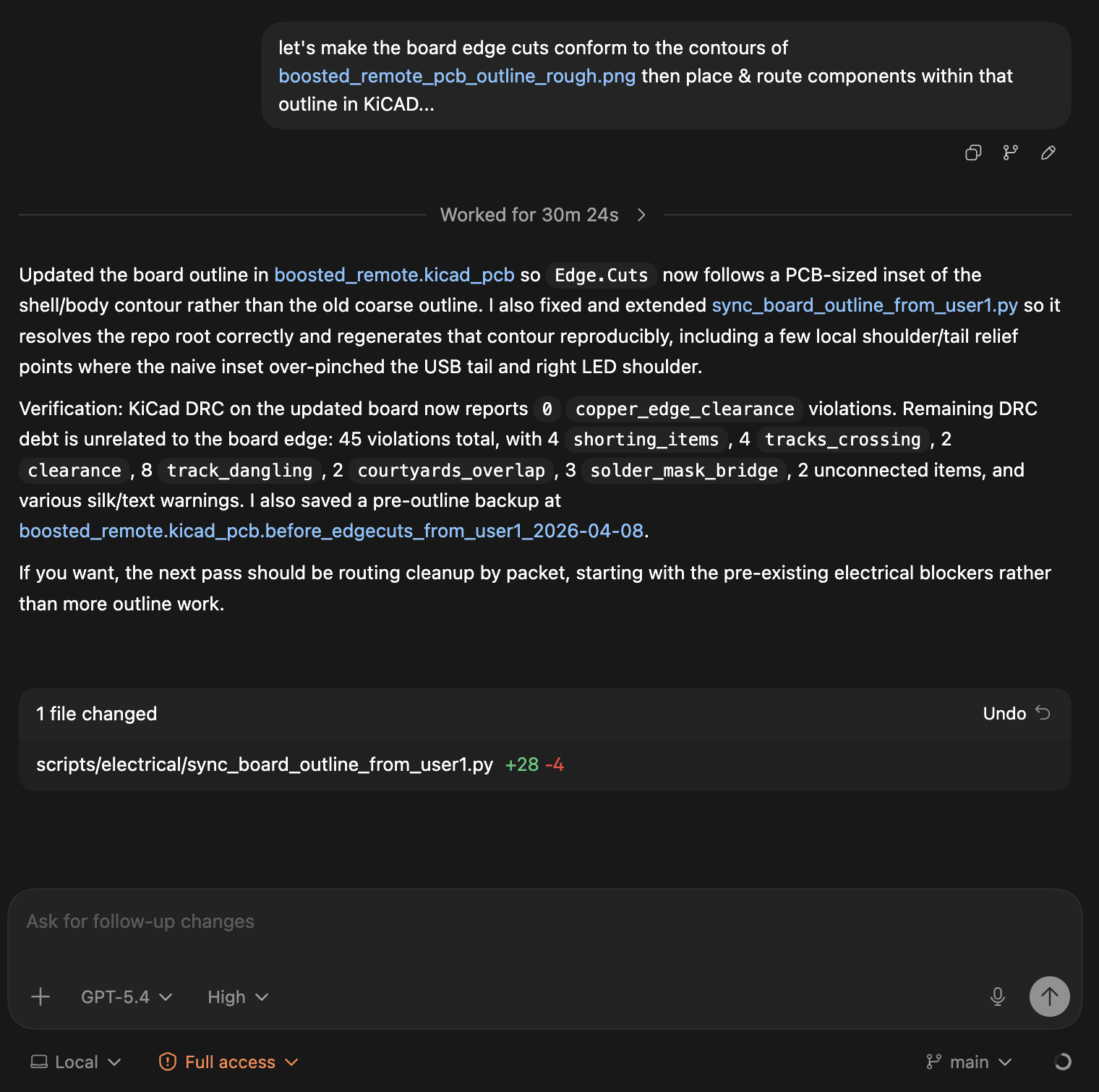
Prompt Snippets
My prompting style is pretty ad hoc and seat-of-my-pants, but here's a few screenshots from actual sessions.


Key Takeaways
Agents Can Accelerate the PCB Design and EDA Process Leveraging programmatic EDA tools such as electrical rule checkers (ERC) and design rule checkers (DRC), Codex was able to iteratively design & implement key aspects of a PCB design project including design specification, component selection, electrical schematic generation, copper routing including vias, placements, and drill guides to wire everything up on the board. As tempting as it would be to say Codex "one-shotted" this, in reality, there was a ton of back and forth between me and the model. With all things AI, your mileage may vary, but I suspect a seasoned circuit designer using a similar approach would be able to take this even further.
Design for Manufacture & Testing Design for Manufacturability (DFM) and Testing (DFT), and other industry standard practices (ergonomics, industrial design, etc.) can be included in the original prompt to help round-out the agents thinking to include more than just electrical engineering.
Proper Placement is Half the Battle As I learned from a number of dead-end routing jobs, a well laid-out board is a board half-routed. I seemed to get the best results when I approached the design hierarchically - starting with the board sides and outline, and moving into mounting holes, large components, traces, and channels, all the way down to the tiny resisters, diodes, and capacitors. When the board was sensibly laid out, and the schematic is properly validated, the routing became much easier.
Caveats
Passing electrical & design rule checks in software doesn't mean the board works. In fact, I'm pretty sure it doesn't for a variety of electrical (and mechanical) reasons. The screenshots in this write-up are missing the board and remote battery LEDs, the buzzer, and the mounting holes don't line up with the original shell.
Areas for Improvement
- Proper part measurements with callipers
- Bluetooth firmware and motor actuators
- Filling in the shell's gaps and proper punch outs for the throttle wheel, trigger, charge port, and LED indicators.
Resources
Built With
- codex
- kicad
- python

Log in or sign up for Devpost to join the conversation.