-
-
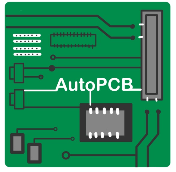
AutoPCB logo
-
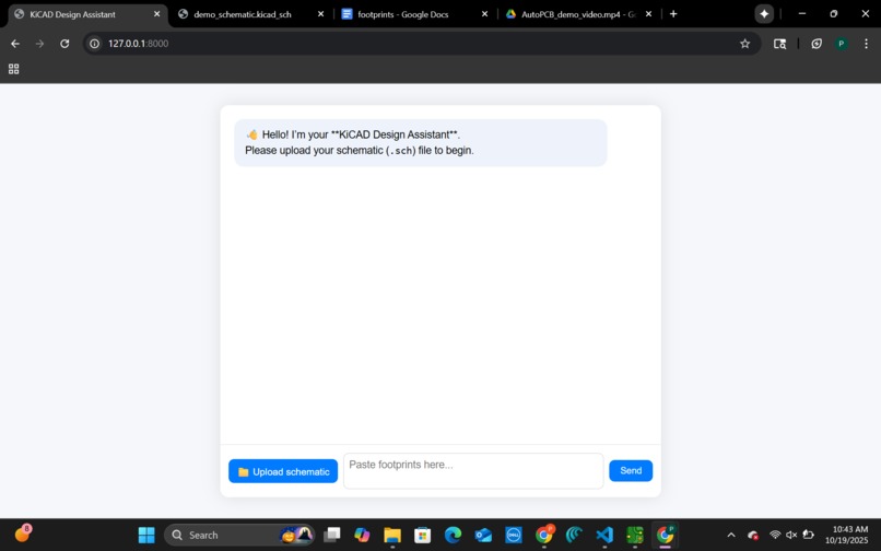
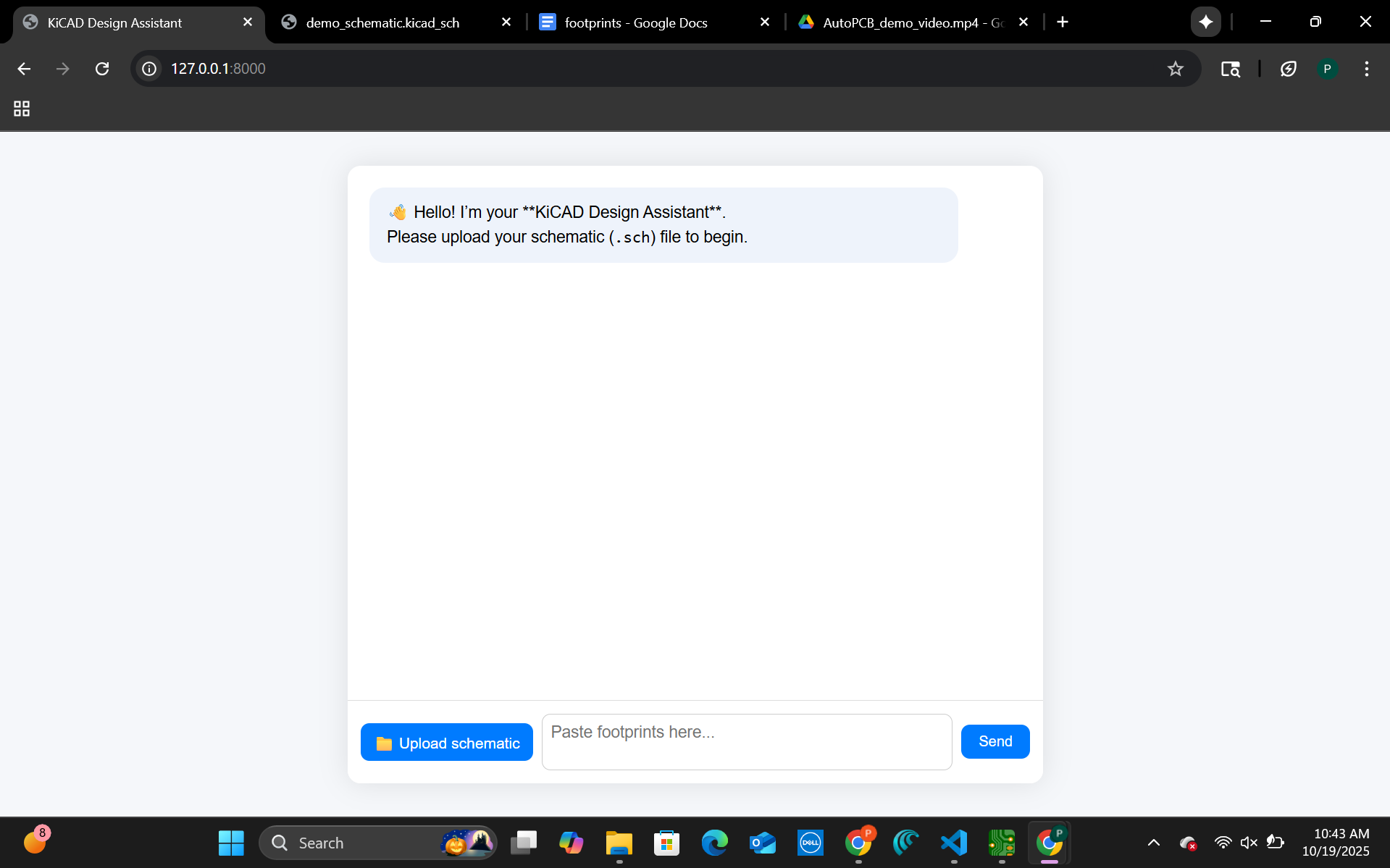
Welcome Screen: The KiCad Design Assistant greets the user and prompts for a schematic upload.
-

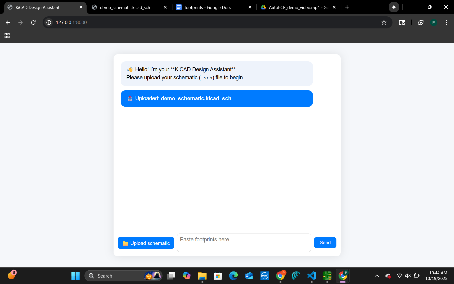
File Upload: The user uploads the schematic file to begin automatic PCB generation.
-
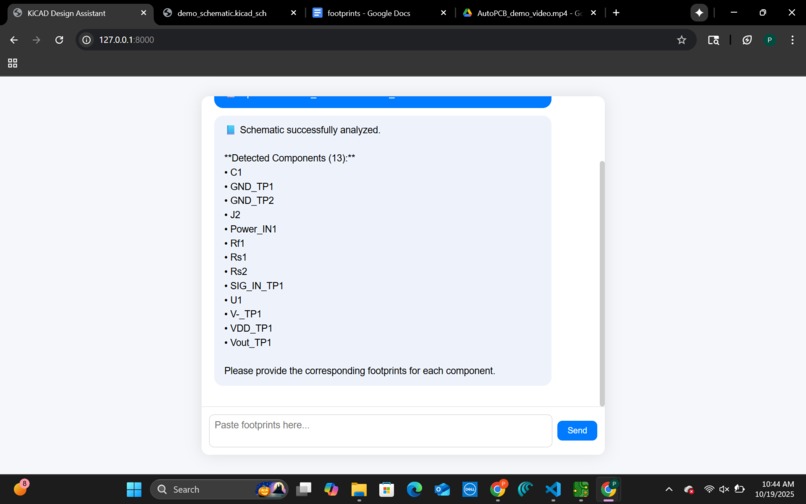
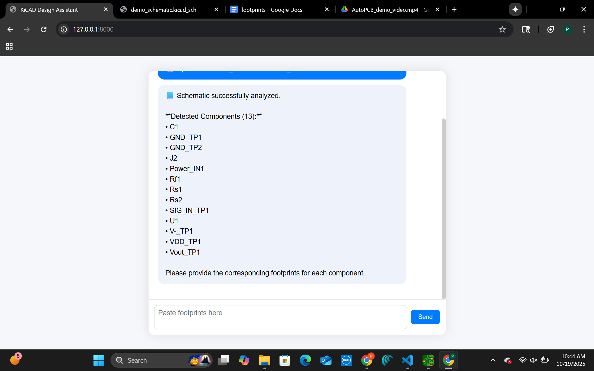
Component Detection: AutoPCB parses the schematic and lists all detected components.
-
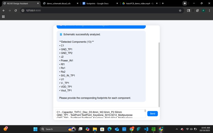
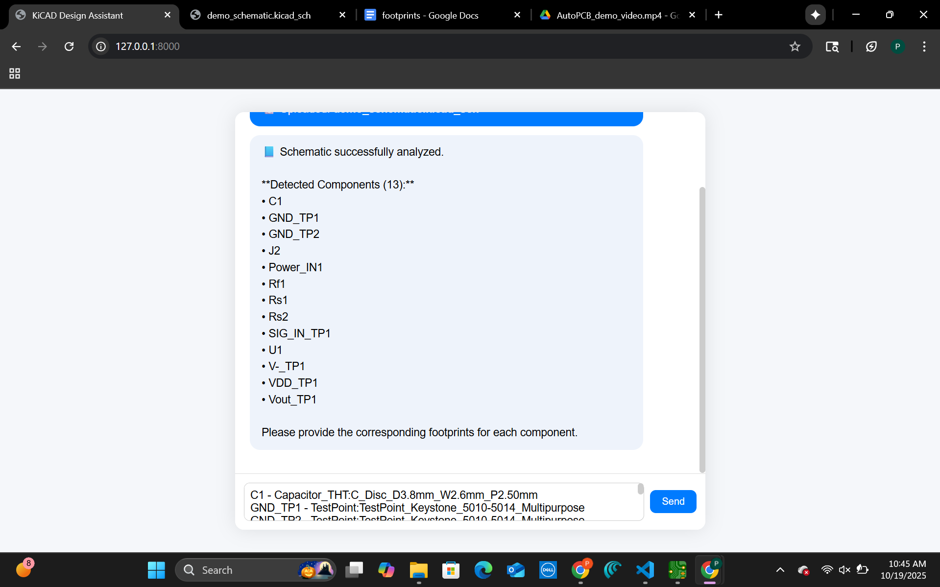
Footprint Assignment: The user assigns footprints for each detected component.
-
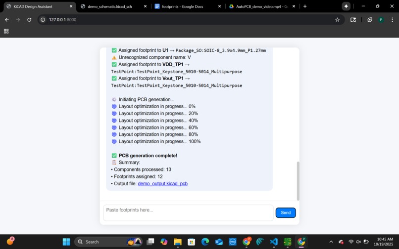
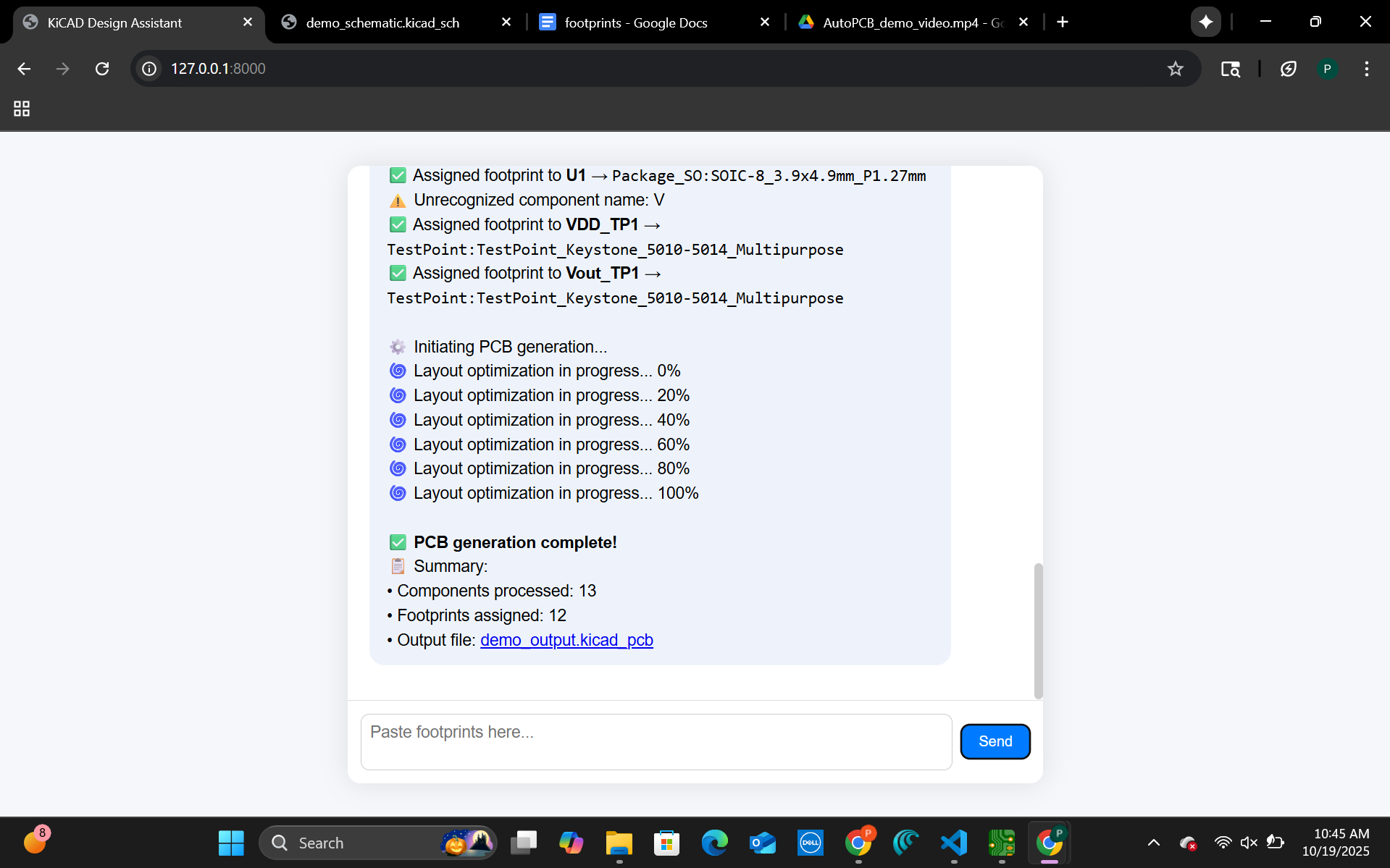
PCB Generation: AutoPCB runs layout optimization and generates the PCB automatically.
-
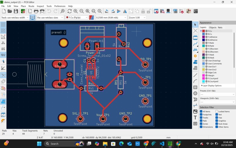
Final Output: The completed, AI-generated PCB layout is displayed in KiCad.


🧠 Inspiration
Designing PCBs is a tedious and error-prone process. Translating a schematic into a physical layout involves repetitive manual steps like assigning footprints, tracing nets, and verifying connections. We wanted to build a tool that makes PCB design more accessible and automated — bridging the gap between circuit ideas and manufacturable boards.
⚙️ What it does
AutoPCB is a proof of concept that automatically converts electrical schematics into PCB layouts. It uses AI-assisted net inference and component recognition to parse circuit diagrams, assign footprints, and generate preliminary KiCad board files — showing what a fully automated schematic-to-PCB pipeline could look like.
🛠️ How we built it
We combined Python, FastAPI, and the KiCad 9.0 API to demonstrate the concept. The backend parses schematics, performs net inference using the Gemini API, and assigns component footprints. While not yet a fully functional tool, our prototype outlines the complete workflow and architecture needed to make AutoPCB production-ready.
🚧 Challenges we ran into
- Integrating the KiCad Python API across platforms.
- Parsing inconsistent schematic formats (.sch, .kicad_sch).
- Handling incomplete footprint and net data.
- Debugging environment issues between Windows and WSL.
🏆 Accomplishments we’re proud of
- Created a working prototype that demonstrates the concept of automated schematic-to-PCB conversion.
- Achieved successful AI-driven net inference using the Gemini API.
- Built a clear pipeline integrating FastAPI, AI inference, and KiCad.
- Gained insight into how automation can significantly speed up PCB workflows.
💡 What we learned
We learned how intricate PCB workflows are and how much potential there is for automation. We also gained hands-on experience integrating AI models with EDA tools and solving real-world compatibility issues between environments and file formats.
🚀 What’s next for AutoPCB
We know exactly what’s needed to turn this proof of concept into a fully working product:
- Implement schematic image-to-PCB conversion with computer vision.
- Expand component and footprint libraries.
- Add intelligent auto-routing and placement features.
- Build a web-based dashboard for live schematic uploads and interactive PCB previews.


Log in or sign up for Devpost to join the conversation.