-
Overview
Inspiration
AccelScope started with a practical question: how can I explore AI hardware designs and make informed choices without a physical FPGA?
Adding more parallel hardware can reduce processing cycles, but it also uses more logic resources. I wanted to make that tradeoff visible through working circuits, repeatable tests, and a simple interface.
The target users are students and hardware builders who want to understand and verify small accelerator designs before moving to a physical device.
What it does
AccelScope compares two Verilog implementations of the same AI compute building block: a 4×4 matrix-vector multiplication using signed 8-bit inputs and weights.
Users can:
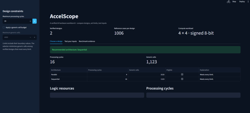
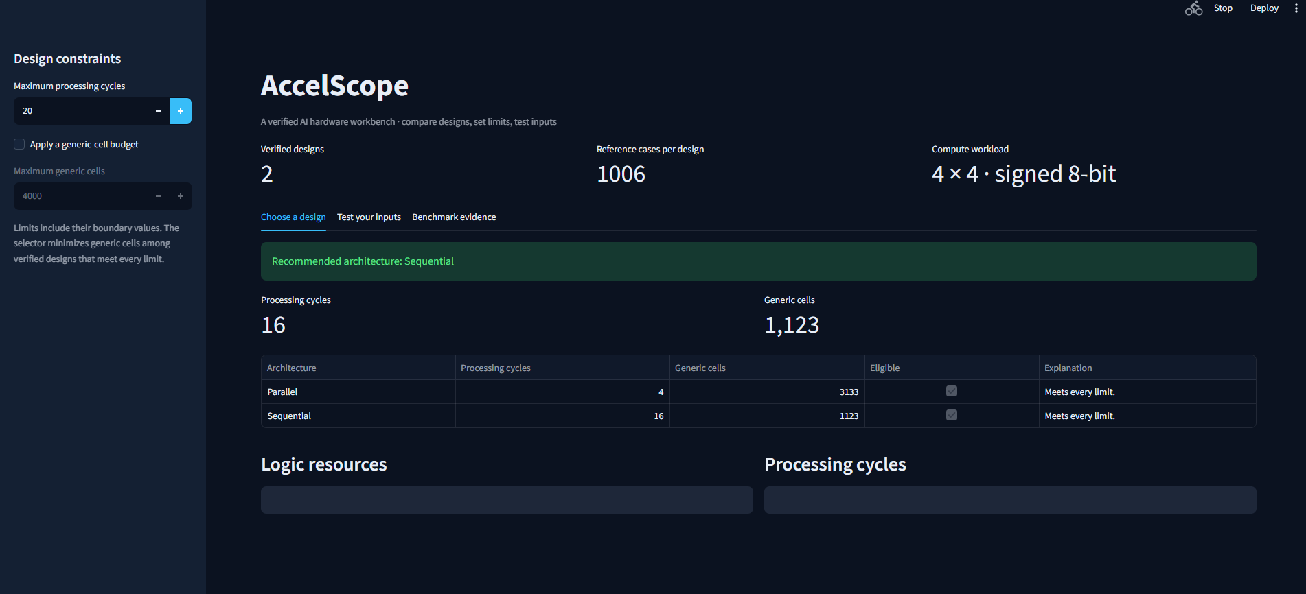
- Compare processing cycles and generic synthesis resources.
- Set a cycle limit and an optional logic-resource budget.
- Choose the verified architecture with the fewest generic cells that meets those limits.
- See why a design was rejected.
- Enter custom inputs and run both hardware simulations against an exact Python reference.
The prototype demonstrates a small arithmetic kernel that can form part of an AI accelerator.
How I built it
I developed AccelScope using Ubuntu under Windows Subsystem for Linux.
First, I created a Python reference model with strict input validation. I then implemented two hardware architectures:
- Sequential: reuses one multiplier to process the calculation over 16 compute cycles.
- Parallel: uses four multipliers to process all four rows concurrently, completing in four compute cycles.
C++ testbenches run the circuits through Verilator. Yosys synthesizes both designs using the same generic flow, allowing their resource counts to be compared.
The Streamlit interface brings the results, constraint selection, and custom-input testing together. Before a live simulation, it checks that the circuit source, testbench, and executable match the saved benchmark evidence.
A single rebuild command runs the tests, compiles both simulations, and regenerates the comparison. GitHub Actions successfully runs this process from a fresh checkout.
Challenges I ran into
Getting signed arithmetic right. Four products of −128 × −128 sum to 65,536. That requires a signed 18-bit accumulator, even though each input is only eight bits.
Interpreting synthesis results correctly. Dynamic output indexing introduced an incidental multiplication into the sequential design’s synthesis representation. Replacing it with explicit output assignments made the high-level multiplier count reflect the intended arithmetic hardware.
Testing control behavior as well as arithmetic. Correct numerical results alone were insufficient. The testbenches also check captured inputs, ignored start requests during processing, completion pulses, retained outputs, and recovery after reset.
Accomplishments I’m proud of
Both designs passed 1,006 Python-reference cases, alongside protocol and reset checks. All 27 Python tests passed locally and in GitHub Actions.
The recorded synthesis comparison is:
| Architecture | Compute cycles | High-level multipliers | Generic cells |
|---|---|---|---|
| Sequential | 16 | 1 | 1,123 |
| Parallel | 4 | 4 | 3,133 |
The interface also successfully ran both hardware simulations on custom inputs, matching the expected outputs: 30, −30, 10, and −4.
The selector demonstrates a useful decision process: a 16-cycle limit favors Sequential, an eight-cycle limit selects Parallel, and an eight-cycle limit combined with a 2,000-cell budget correctly reports that neither supported design qualifies.
What I learned
I learned how parallelism changes the balance between computation cycles and logic resources, and how important explicit widths and signed values are in hardware design.
I also learned to distinguish measurements carefully. Four times fewer compute cycles does not establish four times faster execution. Clock frequency, physical area, and power remain unmeasured. Generic synthesis cells describe the recorded tool flow rather than physical chip area or device-specific FPGA resources.
What’s next for AccelScope
I want to add more verified architectures, support larger workloads, and map the circuits to a specific FPGA. Timing analysis, device-specific resource measurements, and memory-transfer costs would make future recommendations more useful.

Log in or sign up for Devpost to join the conversation.